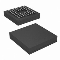
CY7C68053-56BAXIT Cypress Semiconductor Corp, CY7C68053-56BAXIT Datasheet - Page 9

CY7C68053-56BAXIT
Manufacturer Part Number
CY7C68053-56BAXIT
Description
CY7C68053-56BAXIT
Manufacturer
Cypress Semiconductor Corp
Series
MoBL-USB™r
Datasheet
1.CY7C68053-56BAXI.pdf
(42 pages)
Specifications of CY7C68053-56BAXIT
Applications
USB Microcontroller
Core Processor
8051
Program Memory Type
ROMless
Controller Series
CY7C680xx
Ram Size
16K x 8
Interface
I²C, USB
Number Of I /o
56
Voltage - Supply
1.71 V ~ 1.89 V
Operating Temperature
-40°C ~ 85°C
Mounting Type
Surface Mount
Package / Case
56-VFBGA
Processor Series
CY7C68xx
Core
8051
Data Bus Width
8 bit
Data Ram Size
16 KB
Interface Type
I2C
Maximum Clock Frequency
48 MHz
Number Of Programmable I/os
24
Maximum Operating Temperature
+ 85 C
Mounting Style
SMD/SMT
Minimum Operating Temperature
- 40 C
Lead Free Status / RoHS Status
Lead free / RoHS Compliant
For Use With
CY3687 - KIT DEV MOBL-USB FX2LP18
Lead Free Status / Rohs Status
Details
Available stocks
Company
Part Number
Manufacturer
Quantity
Price
Company:
Part Number:
CY7C68053-56BAXIT
Manufacturer:
Cypress Semiconductor Corp
Quantity:
10 000
3.12.6 Default High Speed Alternate Settings
Table 5. Default High Speed Alternate Settings
3.13 External FIFO Interface
The architecture, control signals, and clock rates are presented
in this section.
3.13.1 Architecture
The FX2LP18 slave FIFO architecture has eight 512-byte blocks
in the endpoint RAM that directly serve as FIFO memories and
are controlled by FIFO control signals (such as IFCLK, SLCS#,
SLRD, SLWR, SLOE, PKTEND, and flags).
In operation, some of the eight RAM blocks fill or empty from the
SIE while the others are connected to the I/O transfer logic. The
transfer logic takes two forms: the GPIF for internally generated
control signals or the slave FIFO interface for externally
controlled transfers.
3.13.2 Master/Slave Control Signals
The FX2LP18 endpoint FIFOs are implemented as eight
physically distinct 256x16 RAM blocks. The 8051/SIE can switch
any of the RAM blocks between two domains, the USB (SIE)
domain and the 8051-I/O Unit domain. This switching is
instantaneous, giving zero transfer time between ‘USB FIFOs’
and ‘Slave FIFOs’. Because they are physically the same
memory, no bytes are actually transferred between buffers.
At any given time, some RAM blocks are filling and emptying with
USB data under SIE control, while other RAM blocks are
available to the 8051, the I/O control unit, or both. The RAM
blocks operate as single port in the USB domain, and dual port
in the 8051-I/O domain. The blocks can be configured as single,
double, triple, or quad buffered as previously shown.
The I/O control unit implements either an internal master (M for
master) or external master (S for Slave) interface.
In Master (M) mode, the GPIF internally controls FIFOADR[1:0]
to select a FIFO. The two ready (RDY) pins can be used as flag
inputs from an external FIFO or other logic. The GPIF can be run
from either an internally derived clock or externally supplied
clock (IFCLK), at a rate that transfers data up to 96 megabytes/s
(48 MHz IFCLK with 16-bit interface).
Document # 001-06120 Rev *J
Note
ep0
ep1out
ep1in
ep2
ep4
ep6
ep8
5. Even though these buffers are 64 bytes, they are reported as 512 for USB 2.0 compliance. Nnever transfer packets larger than 64 bytes to EP1.
Alternate Setting
64
0
0
0
0
0
0
0
64
512 bulk
512 bulk
512 bulk in (2×)
512 bulk out (2×)
512 bulk out (2×)
512 bulk in (2×)
[3, 4]
[5]
[5]
1
In Slave (S) mode, the FX2LP18 accepts either an internally
derived clock or externally supplied clock (IFCLK, maximum
frequency 48 MHz) and SLCS#, SLRD, SLWR, SLOE, PKTEND
signals from external logic. When using an external IFCLK, the
external clock must be present before switching to the external
clock with the IFCLKSRC bit. Each endpoint can individually be
selected for byte or word operation by an internal configuration
bit, and a Slave FIFO Output Enable signal (SLOE) enables data
of the selected width. External logic must insure that the output
enable signal is inactive when writing data to a slave FIFO. The
slave interface can also operate asynchronously, where the
SLRD and SLWR signals act directly as strobes, rather than a
clock qualifier as in synchronous mode. The signals SLRD,
SLWR, SLOE, and PKTEND are gated by the signal SLCS#.
3.13.3 GPIF and FIFO Clock Rates
An 8051 register bit selects one of two frequencies for the
internally supplied interface clock: 30 MHz and 48 MHz.
Alternatively, an externally supplied clock of 5 MHz–48 MHz
feeding the IFCLK pin can be used as the interface clock. IFCLK
can be configured to function as an output clock when the GPIF
and FIFOs are internally clocked. An output enable bit in the
IFCONFIG register turns this clock output off. Another bit within
the IFCONFIG register inverts the IFCLK signal whether
internally or externally sourced.
3.14 GPIF
The GPIF is a flexible 8- or 16-bit parallel interface driven by a
user programmable finite state machine. It allows the
CY7C68053 to perform local bus mastering, and can implement
a wide variety of protocols such as ATA interface, parallel printer
port, and Utopia.
The GPIF has three programmable control outputs (CTL), and
two general purpose ready inputs.The data bus width can be 8
or 16 bits. Each GPIF vector defines the state of the control
outputs, and determines what state a ready input (or multiple
inputs) must be before proceeding. The GPIF vector can be
programmed to advance a FIFO to the next data value, advance
an address, and so on. A sequence of the GPIF vectors makes
up a single waveform that is executed to perform the desired
data move between the FX2LP18 and the external device.
64
64 int
64 int
512 int out (2×)
512 bulk out (2×)
512 int in (2×)
512 bulk in (2×)
2
64
64 int
64 int
512 iso out (2×)
512 bulk out (2×)
512 iso in (2×)
512 bulk in (2×)
CY7C68053
3
Page 9 of 42
[+] Feedback


