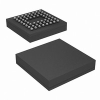
CY7C68053-56BAXIT Cypress Semiconductor Corp, CY7C68053-56BAXIT Datasheet - Page 6

CY7C68053-56BAXIT
Manufacturer Part Number
CY7C68053-56BAXIT
Description
CY7C68053-56BAXIT
Manufacturer
Cypress Semiconductor Corp
Series
MoBL-USB™r
Datasheet
1.CY7C68053-56BAXI.pdf
(42 pages)
Specifications of CY7C68053-56BAXIT
Applications
USB Microcontroller
Core Processor
8051
Program Memory Type
ROMless
Controller Series
CY7C680xx
Ram Size
16K x 8
Interface
I²C, USB
Number Of I /o
56
Voltage - Supply
1.71 V ~ 1.89 V
Operating Temperature
-40°C ~ 85°C
Mounting Type
Surface Mount
Package / Case
56-VFBGA
Processor Series
CY7C68xx
Core
8051
Data Bus Width
8 bit
Data Ram Size
16 KB
Interface Type
I2C
Maximum Clock Frequency
48 MHz
Number Of Programmable I/os
24
Maximum Operating Temperature
+ 85 C
Mounting Style
SMD/SMT
Minimum Operating Temperature
- 40 C
Lead Free Status / RoHS Status
Lead free / RoHS Compliant
For Use With
CY3687 - KIT DEV MOBL-USB FX2LP18
Lead Free Status / Rohs Status
Details
Available stocks
Company
Part Number
Manufacturer
Quantity
Price
Company:
Part Number:
CY7C68053-56BAXIT
Manufacturer:
Cypress Semiconductor Corp
Quantity:
10 000
3.9 Reset and Wakeup
The reset and wakeup pins are described in detail in this section.
3.9.1 Reset Pin
The input pin, RESET#, resets the FX2LP18 when asserted.
This pin has hysteresis and is active LOW. When a crystal is
used with the CY7C68053, the reset period must allow for the
stabilization of the crystal and the PLL. This reset period must be
approximately 5 ms after VCC has reached 3.0 V. If the crystal
input pin is driven by a clock signal the internal PLL stabilizes in
200 μs after V
on reset condition and a reset applied during operation. A power
on reset is defined as the time reset is asserted while power is
being applied to the circuit. A powered reset is defined as a reset
in which the FX2LP18 has previously been powered on and
operating and the RESET# pin is asserted.
Cypress provides an application note which describes and
recommends power on reset implementation, which can be
found on the Cypress web site. For more information on reset
implementation for the MoBL-USB family of products, visit the
Cypress web site at http://www.cypress.com.
Table 3. Reset Timing Values
3.9.2 Wakeup Pins
The 8051 puts itself and the rest of the chip into a power-down
mode by setting PCON.0 = 1. This stops the oscillator and PLL.
When WAKEUP is asserted by external logic, the oscillator
restarts, after the PLL stabilizes, and then the 8051 receives a
wakeup interrupt. This applies whether or not FX2LP18 is
connected to the USB.
Document # 001-06120 Rev *J
Note
Power on reset with crystal
Power on reset with external
clock
Powered reset
2. If the external clock is powered at the same time as the CY7C680xx and has a stabilization wait period, it must be added to the 200 μs.
Figure 2. Reset Timing Plots
RESET#
V
CC
Condition
CC
has reached 3.0 V
T
RESET
200 μs + clock stability time
200 μs
5 ms
Power on Reset
[2]
.
Figure 2
T
RESET
shows a power
V
1.8 V
1.62 V
0 V
IL
The FX2LP18 exits the power down (USB suspend) state using
one of the following methods:
■
■
■
The second wakeup pin, WU2, can also be configured as a
general purpose I/O pin. This allows a simple external R-C
network to be used as a periodic wakeup source. Note that
WAKEUP is active LOW by default.
3.9.3 Lowering Suspend Current
Good design practices for CMOS circuits dictate that any unused
input pins must not be floating between V
input pins will not damage the chip, but can substantially
increase suspend current. To achieve the lowest suspend
current, confiigure unused port pins as outputs. Connect unused
input pins to ground. Some examples of pins that need attention
during suspend are:
■
■
■
RESET#
USB bus activity (if D+/D– lines are left floating, noise on these
lines may indicate activity to the FX2LP18 and initiate a
wakeup)
External logic asserts the WAKEUP pin
External logic asserts the PA3/WU2 pin
Port pins. For Port A, B, D pins, take extra care in shared bus
situations.
❐
❐
❐
CLKOUT. If CLKOUT is not used, it must be tri-stated during
normal operation, but driven during suspend.
IFCLK, RDY0, RDY1. These pins must be pulled to V
GND or driven by another chip.
V
Connect completely unused pins to V
In a single-master system, the firmware must output enable
all the port pins and drive them high or low, before FX2LP18
enters the suspend state.
In a multi-master system (FX2LP18 and another processor
sharing a common data bus), when FX2LP18 is suspended,
the external master must drive the pins high or low. The
external master must not let the pins float.
CC
T
RESET
Powered Reset
IL
CC_IO
and V
CY7C68053
or GND.
1.8 V
0 V
V
IH
Page 6 of 42
IL
. Floating
CC_IO
or
[+] Feedback


