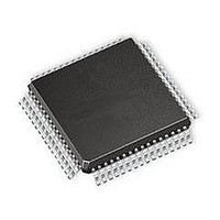
STV2310D STMicroelectronics, STV2310D Datasheet - Page 29

STV2310D
Manufacturer Part Number
STV2310D
Description
Video ICs Digital Video Decodr
Manufacturer
STMicroelectronics
Type
High Quality front end videor
Datasheet
1.STV2310D.pdf
(113 pages)
Specifications of STV2310D
Maximum Operating Temperature
+ 70 C
Package / Case
TQFP-64
Minimum Operating Temperature
0 C
Mounting Style
SMD/SMT
Lead Free Status / RoHS Status
Lead free / RoHS Compliant
Available stocks
Company
Part Number
Manufacturer
Quantity
Price
Company:
Part Number:
STV2310D
Manufacturer:
KEC
Quantity:
2 694
Part Number:
STV2310D
Manufacturer:
ST
Quantity:
20 000
Company:
Part Number:
STV2310D$5R
Manufacturer:
SIGMATEL
Quantity:
20 000
Part Number:
STV2310D$5R
Manufacturer:
ST
Quantity:
20 000
STV2310
4.10.2 Programming
4.11
4.11.1 General Description
Note:
4.11.2 Programming
4.12
4.12.1 General Description
To enable the CrCb overload mechanism, set the CRCBOVER_EN bit in the
The automatic gain for the RGB is set in the
Analog YCrCb Mode
The STV2310 can be programmed in Analog YCrCb mode. This mode has specific input
connections:
A ±20 degree Tint Control mechanism is available to compensate for incorrect hue levels on the
input signals. When the Analog YCrCb mode is programmed, the various clamp circuits are
modified accordingly.
The Fast Blanking (FB) signal is not relevant in Analog YCrCb mode. This mode is a full-page
display mode.
The YCrCb Tint Angle Correction values are programmed in the TINTANGLE[4:0] bits in the
DDECCONT12
coded in 2's complement. The default value is 0 (no correction).
Output FIFO and Line-locked Ouput Pixel Clock Generator
The Output FIFO and Line-Locked Output Pixel Clock Generator block has two functions:
1 Handle the active line data received from the Output Scaler and Format Converter and the
2 Generate the Output Pixel Clock and associated signals.
●
●
●
●
the Y analog input signal must be connected to the CVBS1_Y (or CVBS2_Y) pin
the Cr and Cb analog input signals must be connected to the R_CR and B_CB input pins
(respectively).
ancillary data from the VBI slicer.
The active video line data is provided on 3 buses: Y, Cr and Cb. The output flow is on 8 bit and
multiplexes the Y, Cr and Cb flows. Before being multiplexed, a programmable attenuation can
be applied to the Cr, Cb data. For every output line, digital preambles for synchronization and
ancillary data (when available) are inserted in the output flow in compliance with standard ITU-
R BT 656.
A line-locked output pixel clock is generated. This output clock is a multiple of the input line
frequency. There are 4 possible multiples:
1716 or 1728 in Normal Pixel mode,
1560 or 1888 in Square Pixel mode.
When there is no input signal, the output data can be blanked in option.
When required the STV2310 is able to enlarge the vertical blanking area. On the other hand it
is possible to disable the blanking mode during the VBI, using the "pass through" mode. (The
"pass through" mode must not be selected when the TXT VBI slice is used).
register. The tint angle is coded from -20° to +20° in steps of 1.33°. These bits are
DDECCONT35
register.
Functional Description
DDECCONTB
register.
29/113


