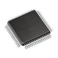
STV2310D STMicroelectronics, STV2310D Datasheet - Page 64

STV2310D
Manufacturer Part Number
STV2310D
Description
Video ICs Digital Video Decodr
Manufacturer
STMicroelectronics
Type
High Quality front end videor
Datasheet
1.STV2310D.pdf
(113 pages)
Specifications of STV2310D
Maximum Operating Temperature
+ 70 C
Package / Case
TQFP-64
Minimum Operating Temperature
0 C
Mounting Style
SMD/SMT
Lead Free Status / RoHS Status
Lead free / RoHS Compliant
Available stocks
Company
Part Number
Manufacturer
Quantity
Price
Company:
Part Number:
STV2310D
Manufacturer:
KEC
Quantity:
2 694
Part Number:
STV2310D
Manufacturer:
ST
Quantity:
20 000
Company:
Part Number:
STV2310D$5R
Manufacturer:
SIGMATEL
Quantity:
20 000
Part Number:
STV2310D$5R
Manufacturer:
ST
Quantity:
20 000
Register List
64/113
MIX_SLOPE[7:0]
Address (hex): 07h
Reset Value (bin): 0000 0000
OUTBUS[7:2]
OUTBUS[1:0]
Address (hex): 08h
Reset Value (bin): 1111 1111
ZOOMIN_FACT
[9:2]
Bit Name
Bit Name
Bit Name
Bit 7
Bit 7
DDECCONT7
DDECCONT8
Bit 6
Bit 6
Soft Mixing Slope, Alpha Blending or Saturated Value
This bitfield provides the soft mixing slope or the alpha blending value depending on Fast Blanking mode.
When the blanking mode is in Forced RGB or Forced CVBS mode, this bitfield is irrelevant.
When the blanking mode is in one of the alpha blending modes, the MIX_SLOPE[7:0] register provides the
alpha value (an FF entry means full scale).
When the blanking mode is in the normal mixing mode between RGB and CVBS, the MIX_SLOPE[1:0] bits
indicate the mixing slope. The MIX_SLOPE[7:2] bits must be set to 000000.
The MIX_SLOPE[1:0] register codes the soft mixing slope from 00 to 11 with 00 corresponding to a slope of
1 clock cycle (4 x f
The default entry is 01, corresponding to a slope of 2 clock cycles.
Alternative values driven by OUTBUS
The OUTBUS[7:2] bits are linked to the HSYNC, VSYNC and FIELD pad control.
When OUTBUS[2] = 0: standard function on HSYNC; when = 1: HSYNC = OUTBUS[3]
When OUTBUS[4] = 0: standard function on VSYNC; when = 1: VSYNC = OUTBUS[5]
When OUTBUS[6] = 0: standard function on FIELD; when = 1: FIELD = OUTBUS[7]
Alternative values driven by OUTBUS
The OUTBUS[1:0] bits are linked to the PLLLOCK pad control.
When OUTBUS[0] = 0: standard function; when = 1: PLLLOCK = OUTBUS[1]
Zoom-in Factor from 1 to 4 (MSBs)
The Zoom-in factor operates from 4 to 1 (No zoom). The LSBs of this value are in the
register. This value must be between 256 (x4) and 1023 (x1).
3FFh: Zoom-in factor of 1 (No zoom) (Default value)
200h: Zoom-in factor of 2
100h: Zoom-in factor of 4 (Enlarged picture)
Bit 5
Bit 5
SC
Register Description
Register Description
clock domain) and 11 corresponding to a slope of 4 clock cycles.
Bit 4
Bit 4
ZOOMIN_FACT[9:2]
OUTBUS[7:0]
Bit 3
Bit 3
Function
Function
Function
Bit 2
Bit 2
Bit 1
Bit 1
DDECCONTB
STV2310
Bit 0
Bit 0


