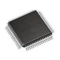
STV2310D STMicroelectronics, STV2310D Datasheet - Page 41

STV2310D
Manufacturer Part Number
STV2310D
Description
Video ICs Digital Video Decodr
Manufacturer
STMicroelectronics
Type
High Quality front end videor
Datasheet
1.STV2310D.pdf
(113 pages)
Specifications of STV2310D
Maximum Operating Temperature
+ 70 C
Package / Case
TQFP-64
Minimum Operating Temperature
0 C
Mounting Style
SMD/SMT
Lead Free Status / RoHS Status
Lead free / RoHS Compliant
Available stocks
Company
Part Number
Manufacturer
Quantity
Price
Company:
Part Number:
STV2310D
Manufacturer:
KEC
Quantity:
2 694
Part Number:
STV2310D
Manufacturer:
ST
Quantity:
20 000
Company:
Part Number:
STV2310D$5R
Manufacturer:
SIGMATEL
Quantity:
20 000
Part Number:
STV2310D$5R
Manufacturer:
ST
Quantity:
20 000
STV2310
4.12.4 Line-Locked Output Pixel Clock Generation
4.12.5 Alternate Functions: Bus Extensions
4.12.6 Output Code Clipping
4.12.7 Programming
The ancillary data is always inserted between the EAV and SAV codes of each line.
The line number is provided by the VBI slicer.VBI data is inserted on the next possible output line.
The only lines where insertion cannot take place are the forbidden lines. The list of forbidden lines
depend on the standard:
Ancillary data is inserted starting just after the EAV code. Ancillary data will replace the blanking
data codes. Ancillary data is inserted in the same order as it is received from the VBI slicer.
VBI data belonging to the same line at reception is inserted in a single line.The maximum number of
ancillary data bytes to be inserted is 84.
A phase-locked loop (PLL) generates a clock signal (CLK_DATA) that is used to read the output
FIFO and to output the YCrCb data in synchronization. This output pixel clock frequency is a
multiple of the input line frequency. Its value (1716, 1728, 1560 or 1888) depends on the input TV
standard and the programmable Normal Pixel or Square Pixel mode.
Note that phase jumps detected in the input video are replicated in the output PLL. This is
equivalent to a temporary change of the number of samples per line, but no change in the output
clock frequency. This feature can be disabled. In this case, the output PLL then corrects the input
phase step by frequency modulation.
Output data is issued synchronously to the CLK_DATA clock active edge. Either the rising or falling
edge of the CLK_DATA signal can be programmed as the active edge.
The following pins can be used for bus extension purposes as programmable output pins:
PLLLOCK, HSYNC, VSYNC and FIELD.
PLLLOCK has a second alternate function IRQ (Interrrupt Request). Interrupt can be generated by
several functions described in registers DDECCONT36 and DDECCONT3C.
To allow compatibility with other devices, output codes can be clipped to remain inside 0 to 100% of
luminance (16 to 235) and chrominance (16 to 240) components.
The Vsync Insertion mode for the output flow is selected in the VSYNCTYPE bit in the
DDECCONT0
The PHSHFT_DIS bit in the
the output PLL. By default, phase jumps are allowed when a phase shift in the video input is
transmitted in the data flow to the output PLL.
The active edge for the CLK_DATA signal is selected by the ACTEDGE bit in the
register.
Data is output from the STV2310 on the FIELD, VSYNC, HSYNC, PLLLOCK and YCRCB[7:0] pins
which are synchronous to the CLK_DATA output clock on either the rising or falling edge (depending
on the selected option).
To force the Interlaced output mode, use the NONINTERLACED_EN bit in the
register.
●
●
for the 525 lines (60 Hz): 9,10,11,272,273,274
for the 625 lines (50 Hz): 5,6,7,318,319,320
register.
DDECCONT5
register is used to disable the phase jump mechanism in
Functional Description
DDECCONT18
DDECCONT0
41/113


