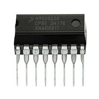
MC9S08QG8CPBE Freescale, MC9S08QG8CPBE Datasheet - Page 119

MC9S08QG8CPBE
Manufacturer Part Number
MC9S08QG8CPBE
Description
Manufacturer
Freescale
Datasheet
1.MC9S08QG8CPBE.pdf
(314 pages)
Specifications of MC9S08QG8CPBE
Cpu Family
HCS08
Device Core Size
8b
Frequency (max)
20MHz
Interface Type
I2C/SCI/SPI
Total Internal Ram Size
512Byte
# I/os (max)
12
Number Of Timers - General Purpose
1
Operating Supply Voltage (typ)
2.5/3.3V
Operating Supply Voltage (max)
3.6V
Operating Supply Voltage (min)
1.8V
On-chip Adc
8-chx10-bit
Instruction Set Architecture
CISC
Operating Temp Range
-40C to 85C
Operating Temperature Classification
Industrial
Mounting
Through Hole
Pin Count
16
Package Type
PDIP
Program Memory Type
Flash
Program Memory Size
8KB
Lead Free Status / RoHS Status
Compliant
Available stocks
Company
Part Number
Manufacturer
Quantity
Price
Company:
Part Number:
MC9S08QG8CPBE
Manufacturer:
CYPRESS
Quantity:
310
- Current page: 119 of 314
- Download datasheet (6Mb)
1
9.1.1
This section provides device-specific information for configuring the ADC on MC9S08QG8/4 devices.
9.1.1.1
The V
V
9.1.1.2
The ADC channel assignments for the MC9S08QG8/4 devices are shown in
convert to an unknown value.
Freescale Semiconductor
ADCH
00000
00001
00010
00011
00100
00101
00110
00111
01000
01001
01010
01011
01100
01101
01110
01111
For information, see
REFL
DDAD
sources for the ADC are internally connected to the V
Channel
AD10
AD11
AD12
AD13
AD14
AD15
AD0
AD1
AD2
AD3
AD4
AD5
AD6
AD7
AD8
AD9
Module Configurations
and V
Analog Supply and Voltage Reference Connections
Channel Assignments
Selecting the internal bandgap channel requires BGBE =1 in SPMSC1; see
Section 5.8.8, “System Power Management Status and Control 1 Register
(SPMSC1).” For the value of the bandgap voltage reference see
Section A.5, “DC
REFH
Section 9.1.1.6, “Temperature
sources for the ADC are internally connected to the V
PTA0/ADP0
PTA1/ADP1
PTA2/ADP2
PTA3/ADP3
PTB0/ADP4
PTB1/ADP5
PTB2/ADP6
PTB3/ADP7
Input
V
V
V
V
V
V
V
V
SS
SS
SS
SS
SS
SS
SS
SS
MC9S08QG8 and MC9S08QG4 Data Sheet, Rev. 5
Characteristics.”
Table 9-1. ADC Channel Assignment
Pin Control
Sensor.”
ADPC0
ADPC1
ADPC2
ADPC3
ADPC4
ADPC5
ADPC6
ADPC7
N/A
N/A
N/A
N/A
N/A
N/A
N/A
N/A
NOTE
ADCH
10000
10001
10010
10011
10100
10101
10110
10111
11000
11001
11010
11011
11100
11101
11110
11111
SS
Chapter 9 Analog-to-Digital Converter (S08ADC10V1)
pin.
Channel
Disabled
Module
V
V
AD16
AD17
AD18
AD19
AD20
AD21
AD22
AD23
AD24
AD25
AD26
AD27
REFH
REFL
—
Table
Internal Bandgap
DD
Temperature
Reserved
Reserved
Reserved
Reserved
Reserved
Sensor
9-1. Reserved channels
pin. The V
Input
None
V
V
V
V
V
V
V
V
SS
SS
SS
SS
SS
SS
DD
SS
1
SSAD
Pin Control
and
N/A
N/A
N/A
N/A
N/A
N/A
N/A
N/A
N/A
N/A
N/A
N/A
N/A
N/A
N/A
N/A
117
Related parts for MC9S08QG8CPBE
Image
Part Number
Description
Manufacturer
Datasheet
Request
R

Part Number:
Description:
TOWER ELEVATOR BOARDS HARDWARE
Manufacturer:
Freescale Semiconductor
Datasheet:

Part Number:
Description:
TOWER SERIAL I/O HARDWARE
Manufacturer:
Freescale Semiconductor
Datasheet:

Part Number:
Description:
LCD MODULE FOR TWR SYSTEM
Manufacturer:
Freescale Semiconductor
Datasheet:

Part Number:
Description:
DAUGHTER LCD WVGA I.MX51
Manufacturer:
Freescale Semiconductor
Datasheet:

Part Number:
Description:
TOWER SYSTEM BOARD MPC5125
Manufacturer:
Freescale Semiconductor
Datasheet:

Part Number:
Description:
KIT EVALUATION I.MX51
Manufacturer:
Freescale Semiconductor
Datasheet:

Part Number:
Description:
KIT DEVELOPMENT WINCE IMX25
Manufacturer:
Freescale Semiconductor
Datasheet:

Part Number:
Description:
TOWER SYSTEM KIT MPC5125
Manufacturer:
Freescale Semiconductor
Datasheet:

Part Number:
Description:
TOWER SYSTEM BOARD K40X256
Manufacturer:
Freescale Semiconductor
Datasheet:

Part Number:
Description:
TOWER SYSTEM KIT K40X256
Manufacturer:
Freescale Semiconductor
Datasheet:

Part Number:
Description:
Microcontrollers (MCU) MX28 PLATFORM DEV KIT
Manufacturer:
Freescale Semiconductor
Datasheet:

Part Number:
Description:
MCU, MPU & DSP Development Tools IAR KickStart Kit for Kinetis K60
Manufacturer:
Freescale Semiconductor
Datasheet:

Part Number:
Description:
24BIT HDMI MX535/08
Manufacturer:
Freescale Semiconductor
Datasheet:
Part Number:
Description:
Manufacturer:
Freescale Semiconductor, Inc
Datasheet:
Part Number:
Description:
Manufacturer:
Freescale Semiconductor, Inc
Datasheet:


