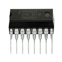
MC9S08QG8CPBE Freescale, MC9S08QG8CPBE Datasheet - Page 200

MC9S08QG8CPBE
Manufacturer Part Number
MC9S08QG8CPBE
Description
Manufacturer
Freescale
Datasheet
1.MC9S08QG8CPBE.pdf
(314 pages)
Specifications of MC9S08QG8CPBE
Cpu Family
HCS08
Device Core Size
8b
Frequency (max)
20MHz
Interface Type
I2C/SCI/SPI
Total Internal Ram Size
512Byte
# I/os (max)
12
Number Of Timers - General Purpose
1
Operating Supply Voltage (typ)
2.5/3.3V
Operating Supply Voltage (max)
3.6V
Operating Supply Voltage (min)
1.8V
On-chip Adc
8-chx10-bit
Instruction Set Architecture
CISC
Operating Temp Range
-40C to 85C
Operating Temperature Classification
Industrial
Mounting
Through Hole
Pin Count
16
Package Type
PDIP
Program Memory Type
Flash
Program Memory Size
8KB
Lead Free Status / RoHS Status
Compliant
Available stocks
Company
Part Number
Manufacturer
Quantity
Price
Company:
Part Number:
MC9S08QG8CPBE
Manufacturer:
CYPRESS
Quantity:
310
- Current page: 200 of 314
- Download datasheet (6Mb)
Serial Communications Interface (S08SCIV3)
14.2.2
This read/write register is used to control various optional features of the SCI system.
198
SCISWAI
SBR[7:0]
Reset
LOOPS
WAKE
RSRC
Field
Field
7:0
ILT
M
7
6
5
4
3
2
W
R
LOOPS
SCI Control Register 1 (SCIC1)
Baud Rate Modulo Divisor — These 13 bits are referred to collectively as BR, and they set the modulo divide
rate for the SCI baud rate generator. When BR = 0, the SCI baud rate generator is disabled to reduce supply
current. When BR = 1 to 8191, the SCI baud rate = BUSCLK/(16×BR). See also BR bits in
Loop Mode Select — Selects between loop back modes and normal 2-pin full-duplex modes. When LOOPS = 1,
the transmitter output is internally connected to the receiver input.
0 Normal operation — RxD and TxD use separate pins.
1 Loop mode or single-wire mode where transmitter outputs are internally connected to receiver input. (See
SCI Stops in Wait Mode
0 SCI clocks continue to run in wait mode so the SCI can be the source of an interrupt that wakes up the CPU.
1 SCI clocks freeze while CPU is in wait mode.
Receiver Source Select — This bit has no meaning or effect unless the LOOPS bit is set to 1. When
LOOPS = 1, the receiver input is internally connected to the TxD pin and RSRC determines whether this
connection is also connected to the transmitter output.
0 Provided LOOPS = 1, RSRC = 0 selects internal loop back mode and the SCI does not use the RxD pins.
1 Single-wire SCI mode where the TxD pin is connected to the transmitter output and receiver input.
9-Bit or 8-Bit Mode Select
0 Normal — start + 8 data bits (LSB first) + stop.
1 Receiver and transmitter use 9-bit data characters
Receiver Wakeup Method Select — Refer to
information.
0 Idle-line wakeup.
1 Address-mark wakeup.
Idle Line Type Select — Setting this bit to 1 ensures that the stop bit and logic 1 bits at the end of a character
do not count toward the 10 or 11 bit times of the logic high level by the idle line detection logic. Refer to
Section 14.3.3.2.1, “Idle-Line
0 Idle character bit count starts after start bit.
1 Idle character bit count starts after stop bit.
0
7
RSRC
start + 8 data bits (LSB first) + 9th data bit + stop.
bit.) RxD pin is not used by SCI.
SCISWAI
0
6
Table 14-2. SCIBDL Register Field Descriptions
Table 14-3. SCIC1 Register Field Descriptions
MC9S08QG8 and MC9S08QG4 Data Sheet, Rev. 5
Figure 14-7. SCI Control Register 1 (SCIC1)
RSRC
Wakeup” for more information.
0
5
M
0
4
Section 14.3.3.2, “Receiver Wakeup
Description
Description
WAKE
3
0
ILT
0
2
Operation” for more
Freescale Semiconductor
PE
0
1
Table
14-1.
PT
0
0
Related parts for MC9S08QG8CPBE
Image
Part Number
Description
Manufacturer
Datasheet
Request
R

Part Number:
Description:
TOWER ELEVATOR BOARDS HARDWARE
Manufacturer:
Freescale Semiconductor
Datasheet:

Part Number:
Description:
TOWER SERIAL I/O HARDWARE
Manufacturer:
Freescale Semiconductor
Datasheet:

Part Number:
Description:
LCD MODULE FOR TWR SYSTEM
Manufacturer:
Freescale Semiconductor
Datasheet:

Part Number:
Description:
DAUGHTER LCD WVGA I.MX51
Manufacturer:
Freescale Semiconductor
Datasheet:

Part Number:
Description:
TOWER SYSTEM BOARD MPC5125
Manufacturer:
Freescale Semiconductor
Datasheet:

Part Number:
Description:
KIT EVALUATION I.MX51
Manufacturer:
Freescale Semiconductor
Datasheet:

Part Number:
Description:
KIT DEVELOPMENT WINCE IMX25
Manufacturer:
Freescale Semiconductor
Datasheet:

Part Number:
Description:
TOWER SYSTEM KIT MPC5125
Manufacturer:
Freescale Semiconductor
Datasheet:

Part Number:
Description:
TOWER SYSTEM BOARD K40X256
Manufacturer:
Freescale Semiconductor
Datasheet:

Part Number:
Description:
TOWER SYSTEM KIT K40X256
Manufacturer:
Freescale Semiconductor
Datasheet:

Part Number:
Description:
Microcontrollers (MCU) MX28 PLATFORM DEV KIT
Manufacturer:
Freescale Semiconductor
Datasheet:

Part Number:
Description:
MCU, MPU & DSP Development Tools IAR KickStart Kit for Kinetis K60
Manufacturer:
Freescale Semiconductor
Datasheet:

Part Number:
Description:
24BIT HDMI MX535/08
Manufacturer:
Freescale Semiconductor
Datasheet:
Part Number:
Description:
Manufacturer:
Freescale Semiconductor, Inc
Datasheet:
Part Number:
Description:
Manufacturer:
Freescale Semiconductor, Inc
Datasheet:


