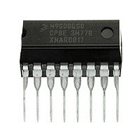
MC9S08QG8CPBE Freescale, MC9S08QG8CPBE Datasheet - Page 50

MC9S08QG8CPBE
Manufacturer Part Number
MC9S08QG8CPBE
Description
Manufacturer
Freescale
Datasheet
1.MC9S08QG8CPBE.pdf
(314 pages)
Specifications of MC9S08QG8CPBE
Cpu Family
HCS08
Device Core Size
8b
Frequency (max)
20MHz
Interface Type
I2C/SCI/SPI
Total Internal Ram Size
512Byte
# I/os (max)
12
Number Of Timers - General Purpose
1
Operating Supply Voltage (typ)
2.5/3.3V
Operating Supply Voltage (max)
3.6V
Operating Supply Voltage (min)
1.8V
On-chip Adc
8-chx10-bit
Instruction Set Architecture
CISC
Operating Temp Range
-40C to 85C
Operating Temperature Classification
Industrial
Mounting
Through Hole
Pin Count
16
Package Type
PDIP
Program Memory Type
Flash
Program Memory Size
8KB
Lead Free Status / RoHS Status
Compliant
Available stocks
Company
Part Number
Manufacturer
Quantity
Price
Company:
Part Number:
MC9S08QG8CPBE
Manufacturer:
CYPRESS
Quantity:
310
- Current page: 50 of 314
- Download datasheet (6Mb)
Chapter 4 Memory Map and Register Definition
4.5.3
The steps for executing any of the commands are listed below. The FCDIV register must be initialized and
any error flags cleared before beginning command execution. The command execution steps are:
A partial command sequence can be aborted manually by writing a 0 to FCBEF any time after the write to
the memory array and before writing the 1 that clears FCBEF and launches the complete command.
Aborting a command in this way sets the FACCERR access error flag, which must be cleared before
starting a new command.
A strictly monitored procedure must be obeyed or the command will not be accepted. This minimizes the
possibility of any unintended changes to the FLASH memory contents. The command complete flag
(FCCF) indicates when a command is complete. The command sequence must be completed by clearing
FCBEF to launch the command.
burst programming. The FCDIV register must be initialized before using any FLASH commands. This
must be done only once following a reset.
48
1. Write a data value to an address in the FLASH array. The address and data information from this
2. Write the command code for the desired command to FCMD. The five valid commands are blank
3. Write a 1 to the FCBEF bit in FSTAT to clear FCBEF and launch the command (including its
write is latched into the FLASH interface. This write is a required first step in any command
sequence. For erase and blank check commands, the value of the data is not important. For page
erase commands, the address may be any address in the 512-byte page of FLASH to be erased. For
mass erase and blank check commands, the address can be any address in the FLASH memory.
Whole pages of 512 bytes are the smallest block of FLASH that may be erased.
check (0x05), byte program (0x20), burst program (0x25), page erase (0x40), and mass erase
(0x41). The command code is latched into the command buffer.
address and data information).
Program and Erase Command Execution
Do not program any byte in the FLASH more than once after a successful
erase operation. Reprogramming bits to a byte that is already programmed
is not allowed without first erasing the page in which the byte resides or
mass erasing the entire FLASH memory. Programming without first erasing
may disturb data stored in the FLASH.
MC9S08QG8 and MC9S08QG4 Data Sheet, Rev. 5
Figure 4-2
is a flowchart for executing all of the commands except for
NOTE
Freescale Semiconductor
Related parts for MC9S08QG8CPBE
Image
Part Number
Description
Manufacturer
Datasheet
Request
R

Part Number:
Description:
TOWER ELEVATOR BOARDS HARDWARE
Manufacturer:
Freescale Semiconductor
Datasheet:

Part Number:
Description:
TOWER SERIAL I/O HARDWARE
Manufacturer:
Freescale Semiconductor
Datasheet:

Part Number:
Description:
LCD MODULE FOR TWR SYSTEM
Manufacturer:
Freescale Semiconductor
Datasheet:

Part Number:
Description:
DAUGHTER LCD WVGA I.MX51
Manufacturer:
Freescale Semiconductor
Datasheet:

Part Number:
Description:
TOWER SYSTEM BOARD MPC5125
Manufacturer:
Freescale Semiconductor
Datasheet:

Part Number:
Description:
KIT EVALUATION I.MX51
Manufacturer:
Freescale Semiconductor
Datasheet:

Part Number:
Description:
KIT DEVELOPMENT WINCE IMX25
Manufacturer:
Freescale Semiconductor
Datasheet:

Part Number:
Description:
TOWER SYSTEM KIT MPC5125
Manufacturer:
Freescale Semiconductor
Datasheet:

Part Number:
Description:
TOWER SYSTEM BOARD K40X256
Manufacturer:
Freescale Semiconductor
Datasheet:

Part Number:
Description:
TOWER SYSTEM KIT K40X256
Manufacturer:
Freescale Semiconductor
Datasheet:

Part Number:
Description:
Microcontrollers (MCU) MX28 PLATFORM DEV KIT
Manufacturer:
Freescale Semiconductor
Datasheet:

Part Number:
Description:
MCU, MPU & DSP Development Tools IAR KickStart Kit for Kinetis K60
Manufacturer:
Freescale Semiconductor
Datasheet:

Part Number:
Description:
24BIT HDMI MX535/08
Manufacturer:
Freescale Semiconductor
Datasheet:
Part Number:
Description:
Manufacturer:
Freescale Semiconductor, Inc
Datasheet:
Part Number:
Description:
Manufacturer:
Freescale Semiconductor, Inc
Datasheet:


