MC9S08QG8CPBE Freescale, MC9S08QG8CPBE Datasheet - Page 48
MC9S08QG8CPBE
Manufacturer Part Number
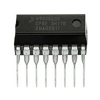
MC9S08QG8CPBE
Description
Manufacturer
Freescale
Datasheet
1.MC9S08QG8CPBE.pdf
(314 pages)
Specifications of MC9S08QG8CPBE
Cpu Family
HCS08
Device Core Size
8b
Frequency (max)
20MHz
Interface Type
I2C/SCI/SPI
Total Internal Ram Size
512Byte
# I/os (max)
12
Number Of Timers - General Purpose
1
Operating Supply Voltage (typ)
2.5/3.3V
Operating Supply Voltage (max)
3.6V
Operating Supply Voltage (min)
1.8V
On-chip Adc
8-chx10-bit
Instruction Set Architecture
CISC
Operating Temp Range
-40C to 85C
Operating Temperature Classification
Industrial
Mounting
Through Hole
Pin Count
16
Package Type
PDIP
Program Memory Type
Flash
Program Memory Size
8KB
Lead Free Status / RoHS Status
Compliant
Available stocks
Company
Part Number
Manufacturer
Quantity
Price
Company:

Part Number:
MC9S08QG8CPBE
Manufacturer:
CYPRESS
Quantity:
310


Chapter 4 Memory Map and Register Definition
4.5
FLASH
The FLASH memory is intended primarily for program storage. In-circuit programming allows the
operating program to be loaded into the FLASH memory after final assembly of the application product.
It is possible to program the entire array through the single-wire background debug interface. Because no
special voltages are needed for FLASH erase and programming operations, in-application programming
is also possible through other software-controlled communication paths. For a more detailed discussion of
in-circuit and in-application programming, refer to the HCS08 Family Reference Manual, Volume I,
Freescale Semiconductor document order number HCS08RMv1/D.
MC9S08QG8 and MC9S08QG4 Data Sheet, Rev. 5
46
Freescale Semiconductor
Related parts for MC9S08QG8CPBE
Image
Part Number
Description
Manufacturer
Datasheet
Request
R

Part Number:
Description:
TOWER ELEVATOR BOARDS HARDWARE
Manufacturer:
Freescale Semiconductor
Datasheet:

Part Number:
Description:
TOWER SERIAL I/O HARDWARE
Manufacturer:
Freescale Semiconductor
Datasheet:

Part Number:
Description:
LCD MODULE FOR TWR SYSTEM
Manufacturer:
Freescale Semiconductor
Datasheet:

Part Number:
Description:
DAUGHTER LCD WVGA I.MX51
Manufacturer:
Freescale Semiconductor
Datasheet:

Part Number:
Description:
TOWER SYSTEM BOARD MPC5125
Manufacturer:
Freescale Semiconductor
Datasheet:

Part Number:
Description:
KIT EVALUATION I.MX51
Manufacturer:
Freescale Semiconductor
Datasheet:

Part Number:
Description:
KIT DEVELOPMENT WINCE IMX25
Manufacturer:
Freescale Semiconductor
Datasheet:

Part Number:
Description:
TOWER SYSTEM KIT MPC5125
Manufacturer:
Freescale Semiconductor
Datasheet:

Part Number:
Description:
TOWER SYSTEM BOARD K40X256
Manufacturer:
Freescale Semiconductor
Datasheet:

Part Number:
Description:
TOWER SYSTEM KIT K40X256
Manufacturer:
Freescale Semiconductor
Datasheet:

Part Number:
Description:
Microcontrollers (MCU) MX28 PLATFORM DEV KIT
Manufacturer:
Freescale Semiconductor
Datasheet:

Part Number:
Description:
MCU, MPU & DSP Development Tools IAR KickStart Kit for Kinetis K60
Manufacturer:
Freescale Semiconductor
Datasheet:

Part Number:
Description:
24BIT HDMI MX535/08
Manufacturer:
Freescale Semiconductor
Datasheet:

Part Number:
Description:
Manufacturer:
Freescale Semiconductor, Inc
Datasheet:
Part Number:
Description:
Manufacturer:
Freescale Semiconductor, Inc
Datasheet: