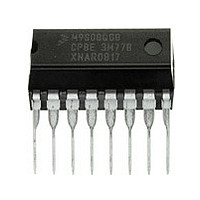
MC9S08QG8CPBE Freescale, MC9S08QG8CPBE Datasheet - Page 278

MC9S08QG8CPBE
Manufacturer Part Number
MC9S08QG8CPBE
Description
Manufacturer
Freescale
Datasheet
1.MC9S08QG8CPBE.pdf
(314 pages)
Specifications of MC9S08QG8CPBE
Cpu Family
HCS08
Device Core Size
8b
Frequency (max)
20MHz
Interface Type
I2C/SCI/SPI
Total Internal Ram Size
512Byte
# I/os (max)
12
Number Of Timers - General Purpose
1
Operating Supply Voltage (typ)
2.5/3.3V
Operating Supply Voltage (max)
3.6V
Operating Supply Voltage (min)
1.8V
On-chip Adc
8-chx10-bit
Instruction Set Architecture
CISC
Operating Temp Range
-40C to 85C
Operating Temperature Classification
Industrial
Mounting
Through Hole
Pin Count
16
Package Type
PDIP
Program Memory Type
Flash
Program Memory Size
8KB
Lead Free Status / RoHS Status
Compliant
Available stocks
Company
Part Number
Manufacturer
Quantity
Price
Company:
Part Number:
MC9S08QG8CPBE
Manufacturer:
CYPRESS
Quantity:
310
- Current page: 278 of 314
- Download datasheet (6Mb)
Appendix A Electrical Characteristics
A.8
This section describes timing characteristics for each peripheral system.
A.8.1
1
2
3
4
5
276
Bus frequency (t
Real-time interrupt internal oscillator period
External reset pulse width
IRQ pulse width
KBIPx pulse width
Port rise and fall time (load = 50 pF)
BKGD/MS setup time after issuing background debug force
reset to enter user or BDM modes
BKGD/MS hold time after issuing background debug force
reset to enter user or BDM modes
Data in Typical column was characterized at 3.0 V, 25°C.
This is the shortest pulse that is guaranteed to be recognized.
This is the minimum pulse width that is guaranteed to pass through the pin synchronization circuitry. Shorter pulses may or
may not be recognized. In stop mode, the synchronizer is bypassed so shorter pulses can be recognized in that case.
Timing is shown with respect to 20% V
To enter BDM mode following a POR, BKGD/MS should be held low during the power-up and for a hold time of t
rises above V
Slew rate control enabled (PTxSE = 1)
Slew rate control disabled (PTxSE = 0)
Asynchronous path
Synchronous path
Asynchronous path
Synchronous path
AC Characteristics
Control Timing
LVD
cyc
.
= 1/f
3
3
2
2
Bus
Parameter
2
)
5
MC9S08QG8 and MC9S08QG4 Data Sheet, Rev. 5
4
DD
and 80% V
Table A-9. Control Timing
DD
levels. Temperature range –40°C to 85°C.
t
t
Symbol
ILIH,
Rise
t
t
MSSU
t
t
f
extrst
t
MSH
ILIH
Bus
RTI
, t
t
IHIL
Fall
1.5 t
1.5 t
Min
700
100
100
100
500
100
—
—
0
cyc
cyc
Typ
1000
30
—
—
—
—
—
—
3
1
Freescale Semiconductor
1300
Max
10
—
—
—
—
—
—
—
MSH
after V
MHz
Unit
μs
ns
ns
ns
ns
ns
μs
DD
Related parts for MC9S08QG8CPBE
Image
Part Number
Description
Manufacturer
Datasheet
Request
R

Part Number:
Description:
TOWER ELEVATOR BOARDS HARDWARE
Manufacturer:
Freescale Semiconductor
Datasheet:

Part Number:
Description:
TOWER SERIAL I/O HARDWARE
Manufacturer:
Freescale Semiconductor
Datasheet:

Part Number:
Description:
LCD MODULE FOR TWR SYSTEM
Manufacturer:
Freescale Semiconductor
Datasheet:

Part Number:
Description:
DAUGHTER LCD WVGA I.MX51
Manufacturer:
Freescale Semiconductor
Datasheet:

Part Number:
Description:
TOWER SYSTEM BOARD MPC5125
Manufacturer:
Freescale Semiconductor
Datasheet:

Part Number:
Description:
KIT EVALUATION I.MX51
Manufacturer:
Freescale Semiconductor
Datasheet:

Part Number:
Description:
KIT DEVELOPMENT WINCE IMX25
Manufacturer:
Freescale Semiconductor
Datasheet:

Part Number:
Description:
TOWER SYSTEM KIT MPC5125
Manufacturer:
Freescale Semiconductor
Datasheet:

Part Number:
Description:
TOWER SYSTEM BOARD K40X256
Manufacturer:
Freescale Semiconductor
Datasheet:

Part Number:
Description:
TOWER SYSTEM KIT K40X256
Manufacturer:
Freescale Semiconductor
Datasheet:

Part Number:
Description:
Microcontrollers (MCU) MX28 PLATFORM DEV KIT
Manufacturer:
Freescale Semiconductor
Datasheet:

Part Number:
Description:
MCU, MPU & DSP Development Tools IAR KickStart Kit for Kinetis K60
Manufacturer:
Freescale Semiconductor
Datasheet:

Part Number:
Description:
24BIT HDMI MX535/08
Manufacturer:
Freescale Semiconductor
Datasheet:
Part Number:
Description:
Manufacturer:
Freescale Semiconductor, Inc
Datasheet:
Part Number:
Description:
Manufacturer:
Freescale Semiconductor, Inc
Datasheet:


