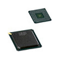
PNX1300EH NXP Semiconductors, PNX1300EH Datasheet - Page 95

PNX1300EH
Manufacturer Part Number
PNX1300EH
Description
Manufacturer
NXP Semiconductors
Datasheet
1.PNX1300EH.pdf
(548 pages)
Specifications of PNX1300EH
Lead Free Status / RoHS Status
Not Compliant
Available stocks
Company
Part Number
Manufacturer
Quantity
Price
Company:
Part Number:
PNX1300EH/G
Manufacturer:
NXP
Quantity:
5 510
Company:
Part Number:
PNX1300EH/G
Manufacturer:
HIT
Quantity:
5 510
Company:
Part Number:
PNX1300EH/G
Manufacturer:
PHILIPS
Quantity:
745
Company:
Part Number:
PNX1300EHG
Manufacturer:
MARVELL
Quantity:
36
- Current page: 95 of 548
- Download datasheet (6Mb)
Philips Semiconductors
for the TIMER CACHE1 source. Event2 selects the
source for TIMER CACHE2.
Table 5-14. Trackable cache-performance events
If the memory bus is available:
• On read data cache miss the minimum waiting time
• On write data cache miss, the missing line needs to
Encoding
14–15
is 12 SDRAM clock cycles, if critical word first is
granted by the Main Memory Interface (MMI). If not,
then data cache waits from 12 to 18 SDRAM cycles
(16 SDRAM cycles are required to fetch 64 bytes
from SDRAM.
be fetched, thus it implies the same SDRAM cycles
as a read data cache miss. If the victimized cache
line is dirty, the cache line is copied back to memory
10
12
13
11
0
1
2
3
4
5
6
7
8
9
No event counted
Instruction-cache misses
Instruction-cache stall cycles (including data-
cache stall cycles if both instruction-cache and
data-cache are stalled simultaneously)
Data-cache bank conflicts
Data-cache read misses
Data-cache write misses
Data-cache stall cycles (that are not also instruc-
tion-cache stall cycles)
Data-cache copyback to SDRAM
Copyback buffer full
Data-cache write miss with all fetch units occu-
pied
Data cache stream miss
Prefetch operation started and not discarded
Prefetch operation discarded (because it hits in
the cache or there is no fetch unit available)
Prefetch operation discarded (because it hits in
the cache)
Reserved
Event
• Prefetch delay is the same as read data cache if
5.8
Table 5-15
eration of PNX1300’s instruction and data caches.
Table 5-15. MMIO register summary
PRELIMINARY SPECIFICATION
DRAM_BASE
DRAM_LIMIT
DRAM_CACHEABLE
_LIMIT
MEM_EVENTS
DC_LOCK_CTL
DC_LOCK_ADDR
DC_LOCK_SIZE
DC_PARAMS
IC_PARAMS
IC_LOCK_CTL
IC_LOCK_ADDR
IC_LOCK_SIZE
MMIO_BASE
after the read of the missing line is done and thus
does not add extra stall cycles.
memory bus is available. As a reminder the prefetch
may be discarded if the data cache state machine is
“full”, and there is a 3 stall cycle penalty when the
prefetch is issued.
MMIO REGISTER SUMMARY
Name
lists the MMIO registers that pertain to the op-
Sets location of the DRAM aperture
Sets size of the DRAM aperture
Divides DRAM aperture into cache-
able and non-cacheable portions
Selects which two events will be
counted by timer/counters
Data-cache locking enable and aper-
ture control
Sets low address of the data-cache
address lock aperture
Sets size of the data-cache address
lock aperture
Read-only register with data-cache
parameter information
Read-only register with instruction-
cache parameter information
Instruction-cache locking enable
Sets low address of the instruction-
cache address lock aperture
Sets size of the instruction-cache
address lock aperture
Sets location of the MMIO aperture
Cache Architecture
Description
5-13
Related parts for PNX1300EH
Image
Part Number
Description
Manufacturer
Datasheet
Request
R
Part Number:
Description:
NXP Semiconductors designed the LPC2420/2460 microcontroller around a 16-bit/32-bitARM7TDMI-S CPU core with real-time debug interfaces that include both JTAG andembedded trace
Manufacturer:
NXP Semiconductors
Datasheet:

Part Number:
Description:
NXP Semiconductors designed the LPC2458 microcontroller around a 16-bit/32-bitARM7TDMI-S CPU core with real-time debug interfaces that include both JTAG andembedded trace
Manufacturer:
NXP Semiconductors
Datasheet:
Part Number:
Description:
NXP Semiconductors designed the LPC2468 microcontroller around a 16-bit/32-bitARM7TDMI-S CPU core with real-time debug interfaces that include both JTAG andembedded trace
Manufacturer:
NXP Semiconductors
Datasheet:
Part Number:
Description:
NXP Semiconductors designed the LPC2470 microcontroller, powered by theARM7TDMI-S core, to be a highly integrated microcontroller for a wide range ofapplications that require advanced communications and high quality graphic displays
Manufacturer:
NXP Semiconductors
Datasheet:
Part Number:
Description:
NXP Semiconductors designed the LPC2478 microcontroller, powered by theARM7TDMI-S core, to be a highly integrated microcontroller for a wide range ofapplications that require advanced communications and high quality graphic displays
Manufacturer:
NXP Semiconductors
Datasheet:
Part Number:
Description:
The Philips Semiconductors XA (eXtended Architecture) family of 16-bit single-chip microcontrollers is powerful enough to easily handle the requirements of high performance embedded applications, yet inexpensive enough to compete in the market for hi
Manufacturer:
NXP Semiconductors
Datasheet:
Part Number:
Description:
The XA-S3 device is a member of Philips Semiconductors? XA(eXtended Architecture) family of high performance 16-bitsingle-chip microcontrollers
Manufacturer:
NXP Semiconductors
Datasheet:

Part Number:
Description:
The NXP BlueStreak LH75401/LH75411 family consists of two low-cost 16/32-bit System-on-Chip (SoC) devices
Manufacturer:
NXP Semiconductors
Datasheet:

Part Number:
Description:
The NXP LPC3130/3131 combine an 180 MHz ARM926EJ-S CPU core, high-speed USB2
Manufacturer:
NXP Semiconductors
Datasheet:

Part Number:
Description:
The NXP LPC3141 combine a 270 MHz ARM926EJ-S CPU core, High-speed USB 2
Manufacturer:
NXP Semiconductors

Part Number:
Description:
The NXP LPC3143 combine a 270 MHz ARM926EJ-S CPU core, High-speed USB 2
Manufacturer:
NXP Semiconductors

Part Number:
Description:
The NXP LPC3152 combines an 180 MHz ARM926EJ-S CPU core, High-speed USB 2
Manufacturer:
NXP Semiconductors

Part Number:
Description:
The NXP LPC3154 combines an 180 MHz ARM926EJ-S CPU core, High-speed USB 2
Manufacturer:
NXP Semiconductors

Part Number:
Description:
Standard level N-channel enhancement mode Field-Effect Transistor (FET) in a plastic package using NXP High-Performance Automotive (HPA) TrenchMOS technology
Manufacturer:
NXP Semiconductors
Datasheet:


