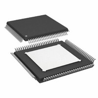
AD9271BSVZRL-25 Analog Devices Inc, AD9271BSVZRL-25 Datasheet - Page 26

AD9271BSVZRL-25
Manufacturer Part Number
AD9271BSVZRL-25
Description
IC ADC OCT 12BIT 25MSPS 100-TQFP
Manufacturer
Analog Devices Inc
Datasheet
1.AD9271BSVZ-50.pdf
(60 pages)
Specifications of AD9271BSVZRL-25
Number Of Bits
12
Sampling Rate (per Second)
25M
Data Interface
Serial, SPI™
Number Of Converters
8
Power Dissipation (max)
1.06W
Voltage Supply Source
Single Supply
Operating Temperature
-40°C ~ 85°C
Mounting Type
Surface Mount
Package / Case
100-TQFP Exposed Pad
Power Dissipation Pd
150mW
Peak Reflow Compatible (260 C)
Yes
Supply Voltage
1.8V
Sample Rate
25 MSPS
Termination Type
SMD
Supply Voltage Max
1.9V
Input Channels Per Adc
8
Lead Free Status / RoHS Status
Lead free / RoHS Compliant
For Use With
AD9271-50EBZ - BOARD EVALUATION AD9271 50MSPS
Lead Free Status / RoHS Status
Lead free / RoHS Compliant, Lead free / RoHS Compliant
Available stocks
Company
Part Number
Manufacturer
Quantity
Price
Company:
Part Number:
AD9271BSVZRL-25
Manufacturer:
AD
Quantity:
1 140
Company:
Part Number:
AD9271BSVZRL-25
Manufacturer:
Analog Devices Inc
Quantity:
10 000
AD9271
Variable Gain Amplifier
The differential X-AMP VGA provides precise input attenuation
and interpolation. It has a low input-referred noise of 4 nV/√Hz
and excellent gain linearity. A simplified block diagram is shown
in Figure 50.
The input of the VGA is a 12-stage differential resistor ladder with
3.01 dB per tap. The resulting total gain range is 30 dB, which
allows for range loss at the endpoints. The effective input resistance
per side is 180 Ω nominally for a total differential resistance of
360 Ω. The ladder is driven by a fully differential input signal from
the LNA. LNA outputs are dc-coupled to avoid external decoupling
capacitors. The common-mode voltage of the attenuator and the
VGA is controlled by an amplifier that uses the same midsupply
voltage derived in the LNA, permitting dc coupling of the LNA
to the VGA without introducing large offsets due to common-
mode differences. However, any offset from the LNA will be
amplified as the gain is increased, producing an exponentially
increasing VGA output offset.
The input stages of the X-AMP are distributed along the ladder,
and a biasing interpolator, controlled by the gain interface,
determines the input tap point. With overlapping bias currents,
signals from successive taps merge to provide a smooth
attenuation range from 0 dB to −30 dB. This circuit technique
results in linear-in-dB gain law conformance and low distortion
levels—only deviating ±0.5 dB or less from the ideal. The gain
GAIN
VIP
VIN
0.450
0.400
0.350
0.300
0.250
0.200
0.150
0.100
0.050
g
m
0
0
LNA GAIN = 5x
LNA
GAIN = 6x
LNA GAIN = 8x
3dB
Figure 49. LNA/VGA Full-Scale Limitations
GAIN INTERPOLATOR
0.1
Figure 50. Simplified VGA Schematic
0.2
0.3
0.4
V
GAIN
0.5
(V)
0.6
0.7
0.8
+
–
POSTAMP
POSTAMP
0.9
1.0
Rev. B | Page 26 of 60
slope is monotonic with respect to the control voltage and is
stable with variations in process, temperature, and supply.
The X-AMP inputs are part of a 24 dB gain feedback amplifier
that completes the VGA. Its bandwidth is about 70 MHz. The
input stage is designed to reduce feedthrough to the output and
to ensure excellent frequency response uniformity across the
gain setting.
Gain Control
The gain control interface, GAIN±, is a differential input. The
VGA gain, V
of all VGAs through the interpolator by selecting the appropriate
input stages connected to the input attenuator. The nominal
V
from about 0.1 V to 0.9 V, where the error is typically less than
±0.5 dB. For V
the error increases. The value of V
voltage by 1 V without gain foldover.
Gain control response time is less than 750 ns to settle within 10%
of the final value for a change from minimum to maximum gain.
There are two ways in which the GAIN+ and GAIN− pins can
be interfaced. Using a single-ended method, a Kelvin type of
connection to ground can be used as shown in Figure 51. For
driving multiple devices, it is preferable to use a differential
method, as shown in Figure 52. In either method, the GAIN+
and GAIN− pins should be dc-coupled and driven to accom-
modate a 1 V full-scale input.
VGA Noise
In a typical application, a VGA compresses a wide dynamic
range input signal to within the input span of an ADC. The
input-referred noise of the LNA limits the minimum resolvable
input signal, whereas the output-referred noise, which depends
primarily on the VGA, limits the maximum instantaneous
dynamic range that can be processed at any one particular gain
control voltage. This latter limit is set in accordance with the
total noise floor of the ADC.
Output-referred noise as a function of V
and Figure 25 for the short-circuit input conditions. The input
GAIN
AD9271
GAIN+
GAIN–
range for 30 dB/V is 0 V to 1 V, with the best gain linearity
AD9271
Figure 51. Single-Ended GAIN± Pins Configuration
GAIN+
GAIN–
Figure 52. Differential GAIN± Pins Configuration
GAIN
GAIN
0.01µF
0.01µF
, is shown in Equation 3. V
100Ω
100Ω
voltages greater than 0.9 V and less than 0.1 V,
±0.25DC AT
±0.25DC AT
0.01µF
0.5V CM
0.5V CM
0.01µF
AD8138
100Ω
CONNECTION
499Ω
499Ω
GAIN
KELVIN
GAIN
can exceed the supply
0.5V CM
523Ω
499Ω
is shown in Figure 24
GAIN
AVDD
50Ω
26kΩ
10kΩ
varies the gain
0 TO 1V DC
50Ω
±0.5V DC


