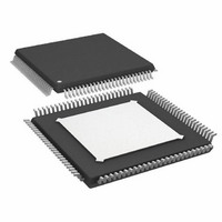
AD9271BSVZRL-25 Analog Devices Inc, AD9271BSVZRL-25 Datasheet - Page 38

AD9271BSVZRL-25
Manufacturer Part Number
AD9271BSVZRL-25
Description
IC ADC OCT 12BIT 25MSPS 100-TQFP
Manufacturer
Analog Devices Inc
Datasheet
1.AD9271BSVZ-50.pdf
(60 pages)
Specifications of AD9271BSVZRL-25
Number Of Bits
12
Sampling Rate (per Second)
25M
Data Interface
Serial, SPI™
Number Of Converters
8
Power Dissipation (max)
1.06W
Voltage Supply Source
Single Supply
Operating Temperature
-40°C ~ 85°C
Mounting Type
Surface Mount
Package / Case
100-TQFP Exposed Pad
Power Dissipation Pd
150mW
Peak Reflow Compatible (260 C)
Yes
Supply Voltage
1.8V
Sample Rate
25 MSPS
Termination Type
SMD
Supply Voltage Max
1.9V
Input Channels Per Adc
8
Lead Free Status / RoHS Status
Lead free / RoHS Compliant
For Use With
AD9271-50EBZ - BOARD EVALUATION AD9271 50MSPS
Lead Free Status / RoHS Status
Lead free / RoHS Compliant, Lead free / RoHS Compliant
Available stocks
Company
Part Number
Manufacturer
Quantity
Price
Company:
Part Number:
AD9271BSVZRL-25
Manufacturer:
AD
Quantity:
1 140
Company:
Part Number:
AD9271BSVZRL-25
Manufacturer:
Analog Devices Inc
Quantity:
10 000
AD9271
Table 15. Memory Map Register
Addr.
(Hex)
Chip Configuration Registers
00
01
02
Device Index and Transfer Registers
04
05
FF
ADC Functions Registers
08
09
Register Name
chip_port_config
chip_id
chip_grade
device_index_2
device_index_1
device_update
modes
clock
X
X
Bit 7
(MSB)
0
X
X
X
X
1
Bit 6
LSB first
1 = on
0 = off
(default)
X
X
X
X
X
X
Child ID [5:4]
(identify device
variants of Chip ID)
00 = 50 MSPS
(default)
01 = 40 MSPS
10 = 25 MSPS
Bit 5
Soft
reset
1 = on
0 = off
(default)
X
Clock
Channel
DCO±
1 = on
0 = off
(default)
X
X
X
(AD9271 = 0x13), (default)
Rev. B | Page 38 of 60
Bit 4
1
X
Clock
Channel
FCO±
1 = on
0 = off
(default)
X
X
X
Chip ID Bits [7:0]
X
Bit 3
1
X
Data
Channel
H
1 = on
(default)
0 = off
Data
Channel
D
1 = on
(default)
0 = off
X
LNA
bypass
1 = on
0 = off
(default)
Bit 2
Soft
reset
1 = on
0 = off
(default)
X
Data
Channel
G
1 = on
(default)
0 = off
Data
Channel
C
1 = on
(default)
0 = off
X
Internal power-down mode
000 = chip run (default)
001 = full power-down
010 = standby
011 = reset
100 = CW mode (TGC PDWN)
X
Bit 1
LSB first
1 = on
0 = off
(default)
X
Data
Channel
F
1 = on
(default)
0 = off
Data
Channel
B
1 = on
(default)
0 = off
X
X
Bit 0
(LSB)
0
X
Data
Channel
E
1 = on
(default)
0 = off
Data
Channel
A
1 = on
(default)
0 = off
SW
transfer
1 = on
0 = off
(default)
Duty cycle
stabilizer
1 = on
(default)
0 = off
Default
Value
0x18
Read
only
0x00
0x0F
0x0F
0x00
0x00
0x01
Notes/
Comments
The nibbles
should be
mirrored so
that LSB- or
MSB-first mode
is set correctly
regardless of
shift mode.
Default is
unique chip ID,
different for
each device.
This is a read-
only register.
Child ID used
to differentiate
graded devices.
Bits are set to
determine
which on-chip
device receives
the next write
command.
Bits are set to
determine
which on-chip
device receives
the next write
command.
Synchronously
transfers data
from the
master shift
register to
the slave.
Determines
various generic
modes of chip
operation.
Turns the
internal duty
cycle stabilizer
on and off.


