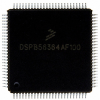
DSPB56364AF100 Freescale Semiconductor, DSPB56364AF100 Datasheet - Page 37

DSPB56364AF100
Manufacturer Part Number
DSPB56364AF100
Description
IC DSP 24BIT AUD 100MHZ 100-LQFP
Manufacturer
Freescale Semiconductor
Series
Symphony™r
Type
Audio Processorr
Datasheet
1.DSPB56364AF100.pdf
(148 pages)
Specifications of DSPB56364AF100
Interface
Host Interface, I²C, SAI, SPI
Clock Rate
100MHz
Non-volatile Memory
ROM (24 kB)
On-chip Ram
11.25kB
Voltage - I/o
3.30V
Voltage - Core
3.30V
Operating Temperature
-40°C ~ 105°C
Mounting Type
Surface Mount
Package / Case
100-LQFP
Lead Free Status / RoHS Status
Lead free / RoHS Compliant
Available stocks
Company
Part Number
Manufacturer
Quantity
Price
Company:
Part Number:
DSPB56364AF100
Manufacturer:
Freescale Semiconductor
Quantity:
135
Company:
Part Number:
DSPB56364AF100
Manufacturer:
TI
Quantity:
996
Company:
Part Number:
DSPB56364AF100
Manufacturer:
Freescale Semiconductor
Quantity:
10 000
Part Number:
DSPB56364AF100
Manufacturer:
FREESCALE
Quantity:
20 000
1
2
3
4
5
6
7
Freescale Semiconductor
No.
147 Last WR assertion to RAS deassertion
148 WR assertion to CAS deassertion
149 Data valid to CAS assertion (write)
150 CAS assertion to data not valid (write)
151 WR assertion to CAS assertion
152 Last RD assertion to RAS deassertion
153 RD assertion to data valid
154 RD deassertion to data not valid
155 WR assertion to data active
156 WR deassertion to data high impedance
The number of wait states for Page mode access is specified in the DCR.
The refresh period is specified in the DCR.
The asynchronous delays specified in the expressions are valid for DSP56364.
There are no DRAMs fast enough to fit to two wait states Page mode @ 100 MHz (See
All the timings are calculated for the worst case. Some of the timings are better for specific cases (e.g., t
read-after-read or write-after-write sequences).
BRW[1:0] (DRAM Control Register bits) defines the number of wait states that should be inserted in each DRAM out-of-page
access.
RD deassertion will always occur after CAS deassertion; therefore, the restricted timing is t
Table 3-10 DRAM Page Mode Timings, Two Wait States
Characteristics
7
DSP56364 Technical Data, Rev. 4.1
Symbol
t
t
t
t
CWL
WCS
ROH
RWL
t
t
t
t
DS
DH
GA
GZ
2.75 × T
0.25 × T
0.25 × T
1.75 × T
1.75 × T
1.75 × T
0.75 × T
2.5 × T
2.5 × T
Expression
0.25 × T
T
C
− 4.3
C
C
C
C
C
C
C
C
C
− 4.3
− 4.0
− 4.3
− 3.7
− 3.0
− 4.0
− 7.5
− 6.5
− 0.3
C
5
External Memory Expansion Port (Port A)
1, 2, 3, 4
33.4
33.6
22.5
10.9
33.9
11.1
Min
0.1
0.0
—
—
—
—
66 MHz
Figure 3-11
OFF
(continued)
Max
19.0
3.8
—
—
—
—
—
—
—
—
—
—
and not t
26.8
27.0
17.9
27.3
).
Min
0.1
8.2
0.0
9.1
—
—
—
—
PC
80 MHz
GZ.
equals 3 × T
Max
15.4
3.1
—
—
—
—
—
—
—
—
—
—
Unit
ns
ns
ns
ns
ns
ns
ns
ns
ns
ns
ns
ns
C
3-21
for


