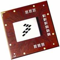
MPC8560PX833LB Freescale Semiconductor, MPC8560PX833LB Datasheet - Page 15

MPC8560PX833LB
Manufacturer Part Number
MPC8560PX833LB
Description
IC MPU POWERQUICC III 783-FCPBGA
Manufacturer
Freescale Semiconductor
Datasheet
1.MPC8560PX833LB.pdf
(104 pages)
Specifications of MPC8560PX833LB
Processor Type
MPC85xx PowerQUICC III 32-Bit
Speed
833MHz
Voltage
1.2V
Mounting Type
Surface Mount
Package / Case
783-FCPBGA
Family Name
MPC85XX
Device Core
PowerQUICC III
Device Core Size
32b
Frequency (max)
833MHz
Instruction Set Architecture
RISC
Supply Voltage 1 (typ)
1.2V
Operating Supply Voltage (max)
1.26V
Operating Supply Voltage (min)
1.14V
Operating Temp Range
0C to 105C
Operating Temperature Classification
Commercial
Mounting
Surface Mount
Pin Count
783
Package Type
FCBGA
For Use With
MPC8560ADS-BGA - BOARD APPLICATION DEV 8560
Lead Free Status / RoHS Status
Contains lead / RoHS non-compliant
Features
-
Lead Free Status / Rohs Status
Not Compliant
Available stocks
Company
Part Number
Manufacturer
Quantity
Price
Company:
Part Number:
MPC8560PX833LB
Manufacturer:
MOTOROLA
Quantity:
852
Company:
Part Number:
MPC8560PX833LB
Manufacturer:
Freescale Semiconductor
Quantity:
10 000
Part Number:
MPC8560PX833LB
Manufacturer:
NXP/恩智浦
Quantity:
20 000
4
4.1
Table 7
Freescale Semiconductor
Notes:
1. GV
2. OV
3. OV
4. V
5. LVDD=2.5/3.3, 15pF load per pin, 25% bus utilization
6. Power dissipation for one TSEC only
7. OV
TDMA or TDMB
SYSCLK frequency
SYSCLK cycle time
SYSCLK rise and fall time
SYSCLK duty cycle
SYSCLK jitter
Notes:
1. Caution: The CCB to SYSCLK ratio and e500 core to CCB ratio settings must be chosen such that the resulting SYSCLK
2. Rise and fall times for SYSCLK are measured at 0.6 V and 2.7 V.
3. Timing is guaranteed by design and characterization.
4. This represents the total input jitter—short term and long term—and is guaranteed by design.
5. For spread spectrum clocking, guidelines are +/-1% of the input frequency with a maximum of 60 kHz of modulation
load on clock
frequency, e500 (core) frequency, and CCB frequency do not exceed their respective maximum or minimum operating
frequencies. Refer to
regardless of the input frequency.
Interface
DD
DD
DD
DD
DD
=1.2, OV
=3.3, 30pF load per pin, 54% bus utilization, 33% write cycles
=3.3, 25pF load per pin, 5pF load on clock, 40% bus utilization, 33% write cycles
=3.3, 10pF load per pin, 50% bus utilization
=2.5, ECC enabled, 66% bus utilization, 33% write cycles, 10pF load on data, 10pF load on address/command, 10pF
Clock Timing
provides the system clock (SYSCLK) AC timing specifications for the MPC8560.
System Clock Timing
Parameter/Condition
DD
=3.3
Nibble mode
Per channel
Parameter
Section 15.2, “Platform/System PLL
Table 6. Estimated Typical I/O Power Consumption (continued)
MPC8560 Integrated Processor Hardware Specifications, Rev. 5
Table 7. SYSCLK AC Timing Specifications
GV
DD
—
—
(2.5 V) OV
t
KHKL
Symbol
f
t
t
SYSCLK
SYSCLK
KH
/t
—
, t
SYSCLK
KL
DD
Ratio,” and
10
5
(3.3 V) LV
Min
6.0
0.6
40
—
—
Section 15.3, “e500 Core PLL
DD
—
—
(3.3 V) LV
Typical
1.0
—
—
—
—
DD
—
—
(2.5 V)
+/- 150
Max
166
1.2
60
—
Ratio,” for ratio settings.
Units
mW
MHz
Unit
ns
ns
ps
%
Clock Timing
Notes
Notes
4, 5
7
—
1
2
3
15


