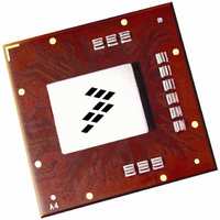
MPC8560PX833LB Freescale Semiconductor, MPC8560PX833LB Datasheet - Page 4

MPC8560PX833LB
Manufacturer Part Number
MPC8560PX833LB
Description
IC MPU POWERQUICC III 783-FCPBGA
Manufacturer
Freescale Semiconductor
Datasheet
1.MPC8560PX833LB.pdf
(104 pages)
Specifications of MPC8560PX833LB
Processor Type
MPC85xx PowerQUICC III 32-Bit
Speed
833MHz
Voltage
1.2V
Mounting Type
Surface Mount
Package / Case
783-FCPBGA
Family Name
MPC85XX
Device Core
PowerQUICC III
Device Core Size
32b
Frequency (max)
833MHz
Instruction Set Architecture
RISC
Supply Voltage 1 (typ)
1.2V
Operating Supply Voltage (max)
1.26V
Operating Supply Voltage (min)
1.14V
Operating Temp Range
0C to 105C
Operating Temperature Classification
Commercial
Mounting
Surface Mount
Pin Count
783
Package Type
FCBGA
For Use With
MPC8560ADS-BGA - BOARD APPLICATION DEV 8560
Lead Free Status / RoHS Status
Contains lead / RoHS non-compliant
Features
-
Lead Free Status / Rohs Status
Not Compliant
Available stocks
Company
Part Number
Manufacturer
Quantity
Price
Company:
Part Number:
MPC8560PX833LB
Manufacturer:
MOTOROLA
Quantity:
852
Company:
Part Number:
MPC8560PX833LB
Manufacturer:
Freescale Semiconductor
Quantity:
10 000
Part Number:
MPC8560PX833LB
Manufacturer:
NXP/恩智浦
Quantity:
20 000
Overview
4
•
•
•
— General-purpose parallel ports—16 parallel I/O lines with interrupt capability
— Supports inverse muxing of ATM cells (IMA)
256 Kbyte L2 cache/SRAM
— Can be configured as follows
— Full ECC support on 64-bit boundary in both cache and SRAM modes
— Cache mode supports instruction caching, data caching, or both
— External masters can force data to be allocated into the cache through programmed memory
— Eight-way set-associative cache organization (1024 sets of 32-byte cache lines)
— Supports locking the entire cache or selected lines. Individual line locks are set and cleared
— Global locking and flash clearing done through writes to L2 configuration registers
— Instruction and data locks can be flash cleared separately
— Read and write buffering for internal bus accesses
— SRAM features include the following:
Address translation and mapping unit (ATMU)
— Eight local access windows define mapping within local 32-bit address space
— Inbound and outbound ATMUs map to larger external address spaces
DDR memory controller
— Programmable timing supporting DDR-1 SDRAM
— 64-bit data interface, up to 333-MHz data rate
— Four banks of memory supported, each up to 1 Gbyte
— DRAM chip configurations from 64 Mbits to 1 Gbit with x8/x16 data ports
— Full ECC support
— Page mode support (up to 16 simultaneous open pages)
– Full cache mode (256-Kbyte cache).
– Full memory-mapped SRAM mode (256-Kbyte SRAM mapped as a single 256-Kbyte
– Half SRAM and half cache mode (128-Kbyte cache and 128-Kbyte memory-mapped
ranges or special transaction types (stashing)
through Book E instructions or by externally mastered transactions
– I/O devices access SRAM regions by marking transactions as snoopable (global)
– Regions can reside at any aligned location in the memory map
– Byte accessible ECC is protected using read-modify-write transactions accesses for smaller
– Three inbound windows plus a configuration window on PCI/PCI-X
– Four inbound windows plus a default and configuration window on RapidIO
– Four outbound windows plus default translation for PCI
– Eight outbound windows plus default translation for RapidIO
block or two 128-Kbyte blocks)
SRAM)
than cache-line accesses.
MPC8560 Integrated Processor Hardware Specifications, Rev. 5
Freescale Semiconductor


