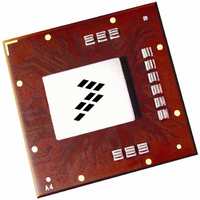
MPC8560PX833LB Freescale Semiconductor, MPC8560PX833LB Datasheet - Page 30

MPC8560PX833LB
Manufacturer Part Number
MPC8560PX833LB
Description
IC MPU POWERQUICC III 783-FCPBGA
Manufacturer
Freescale Semiconductor
Datasheet
1.MPC8560PX833LB.pdf
(104 pages)
Specifications of MPC8560PX833LB
Processor Type
MPC85xx PowerQUICC III 32-Bit
Speed
833MHz
Voltage
1.2V
Mounting Type
Surface Mount
Package / Case
783-FCPBGA
Family Name
MPC85XX
Device Core
PowerQUICC III
Device Core Size
32b
Frequency (max)
833MHz
Instruction Set Architecture
RISC
Supply Voltage 1 (typ)
1.2V
Operating Supply Voltage (max)
1.26V
Operating Supply Voltage (min)
1.14V
Operating Temp Range
0C to 105C
Operating Temperature Classification
Commercial
Mounting
Surface Mount
Pin Count
783
Package Type
FCBGA
For Use With
MPC8560ADS-BGA - BOARD APPLICATION DEV 8560
Lead Free Status / RoHS Status
Contains lead / RoHS non-compliant
Features
-
Lead Free Status / Rohs Status
Not Compliant
Available stocks
Company
Part Number
Manufacturer
Quantity
Price
Company:
Part Number:
MPC8560PX833LB
Manufacturer:
MOTOROLA
Quantity:
852
Company:
Part Number:
MPC8560PX833LB
Manufacturer:
Freescale Semiconductor
Quantity:
10 000
Part Number:
MPC8560PX833LB
Manufacturer:
NXP/恩智浦
Quantity:
20 000
At recommended operating conditions with LV
Ethernet: Three-Speed, MII Management
7.2.4
Table 27
30
Data to clock output skew (at transmitter)
Data to clock input skew (at receiver)
Clock period
Duty cycle for 1000Base-T
Duty cycle for 10BASE-T and 100BASE-TX
Rise and fall time
Notes:
1. Note that, in general, the clock reference symbol representation for this section is based on the symbols RGT to represent
2. The RGMII specification requires that PC board designer add 1.5 ns or greater in trace delay to the RX_CLK in order to meet
3. For 10 and 100 Mbps, t
4. Duty cycle may be stretched/shrunk during speed changes or while transitioning to a received packet's clock domains as long
5. Guaranteed by characterization.
6. Guaranteed by design.
7. Signal timings are measured at 0.5 V and 2.0 V voltage levels.
RGMII and RTBI timing. For example, the subscript of t
notation for rise (R) and fall (F) times follows the clock symbol that is being represented. For symbols representing skews, the
subscript is skew (SK) followed by the clock that is being skewed (RGT).
this specification. However, as stated above, this device will function with only 1.0 ns of delay.
as the minimum duty cycle is not violated and stretching occurs for no more than three t
between.
presents the RGMII and RTBI AC timing specifications.
3
RGMII and RTBI AC Timing
Parameter/Condition
RGT
4
MPC8560 Integrated Processor Hardware Specifications, Rev. 5
scales to 400 ns ± 40 ns and 40 ns ± 4 ns, respectively.
Table 27. RGMII and RTBI AC Timing Specifications
2
DD
of 2.5 V ± 5%.
3
RGT
t
RGTR
t
t
Specifications
RGTH
RGTH
Symbol
t
represents the TBI (T) receive (RX) clock. Note also that the
SKRGT
t
t
SKRGT
RGT
, t
/t
/t
RGTF
RGT
RGT
6
5
1
6
6
6,7
–500
Min
1.0
7.2
45
40
—
RGT
of the lowest speed transitioned
Typ
8.0
50
50
—
—
0
Freescale Semiconductor
Max
0.75
500
2.8
8.8
55
60
Unit
ps
ns
ns
ns
%
%


