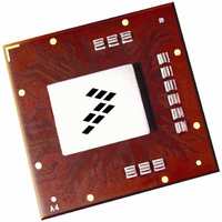
MPC8560PX833LB Freescale Semiconductor, MPC8560PX833LB Datasheet - Page 56

MPC8560PX833LB
Manufacturer Part Number
MPC8560PX833LB
Description
IC MPU POWERQUICC III 783-FCPBGA
Manufacturer
Freescale Semiconductor
Datasheet
1.MPC8560PX833LB.pdf
(104 pages)
Specifications of MPC8560PX833LB
Processor Type
MPC85xx PowerQUICC III 32-Bit
Speed
833MHz
Voltage
1.2V
Mounting Type
Surface Mount
Package / Case
783-FCPBGA
Family Name
MPC85XX
Device Core
PowerQUICC III
Device Core Size
32b
Frequency (max)
833MHz
Instruction Set Architecture
RISC
Supply Voltage 1 (typ)
1.2V
Operating Supply Voltage (max)
1.26V
Operating Supply Voltage (min)
1.14V
Operating Temp Range
0C to 105C
Operating Temperature Classification
Commercial
Mounting
Surface Mount
Pin Count
783
Package Type
FCBGA
For Use With
MPC8560ADS-BGA - BOARD APPLICATION DEV 8560
Lead Free Status / RoHS Status
Contains lead / RoHS non-compliant
Features
-
Lead Free Status / Rohs Status
Not Compliant
Available stocks
Company
Part Number
Manufacturer
Quantity
Price
Company:
Part Number:
MPC8560PX833LB
Manufacturer:
MOTOROLA
Quantity:
852
Company:
Part Number:
MPC8560PX833LB
Manufacturer:
Freescale Semiconductor
Quantity:
10 000
Part Number:
MPC8560PX833LB
Manufacturer:
NXP/恩智浦
Quantity:
20 000
PCI/PCI-X
Table 45
56
PCI-X initialization pattern to HRESET setup time
HRESET to PCI-X initialization pattern hold time
Notes:
1. See the timing measurement conditions in the PCI-X 1.0a Specification.
2. Minimum times are measured at the package pin (not the test point). Maximum times are measured with the test point and
3. Setup time for point-to-point signals applies to REQ and GNT only. All other signals are bused.
4. For purposes of active/float timing measurements, the Hi-Z or off state is defined to be when the total current delivered
5. Setup time applies only when the device is not driving the pin. Devices cannot drive and receive signals at the same time.
6. Maximum value is also limited by delay to the first transaction (time for HRESET high to first configuration access, t
7. A PCI-X device is permitted to have the minimum values shown for t
8. Device must meet this specification independent of how many outputs switch simultaneously.
9. The timing parameter t
10.Guaranteed by characterization.
11.Guaranteed by design.
load circuit.
through the component pin is less than or equal to the leakage current specification.
The PCI-X initialization pattern control signals after the rising edge of HRESET must be negated no later than two clocks
before the first FRAME and must be floated no later than one clock before FRAME is asserted.
mode, the device must meet the requirements specified in PCI 2.2 for the appropriate clock frequency.
Specification.
SYSCLK to signal valid delay
Output hold from SYSCLK
SYSCLK to output high impedance
Input setup time to SYSCLK
Input hold time from SYSCLK
REQ64 to HRESET setup time
HRESET to REQ64 hold time
HRESET high to first FRAME assertion
PCI-X initialization pattern to HRESET setup time
provides the PCI-X AC timing specifications at 133 MHz.
Parameter
Table 44. PCI-X AC Timing Specifications at 66 MHz (continued)
PCRHFV
Parameter
MPC8560 Integrated Processor Hardware Specifications, Rev. 5
Table 45. PCI-X AC Timing Specifications at 133 MHz
is a minimum of 10 clocks rather than the minimum of 5 clocks in the PCI-X 1.0a
t
Symbol
t
t
t
t
t
t
PCKHOV
Symbol
t
t
t
t
PCKHOX
PCKHOZ
PCRVRH
PCRHRX
PCRHFV
PCIVRH
PCIVRH
PCIVKH
PCIXKH
PCRHIX
PCKHOV
Min
and t
0.7
1.4
0.5
10
10
10
—
—
Min
0
10
0
CYC
only in PCI-X mode. In conventional
Max
3.8
50
—
—
—
—
—
—
7
Max
50
—
Freescale Semiconductor
clocks
clocks
clocks
Unit
ns
ns
ns
ns
ns
ns
clocks
Unit
ns
1, 2, 3,
1, 4, 8,
3, 5, 9,
Notes
10, 12
1, 11
7, 8
12
11
11
12
12
12
PCRHFV
Notes
6, 11
11
).


