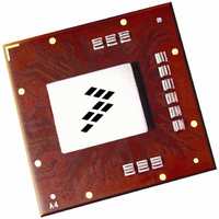
MPC8560PX833LB Freescale Semiconductor, MPC8560PX833LB Datasheet - Page 44

MPC8560PX833LB
Manufacturer Part Number
MPC8560PX833LB
Description
IC MPU POWERQUICC III 783-FCPBGA
Manufacturer
Freescale Semiconductor
Datasheet
1.MPC8560PX833LB.pdf
(104 pages)
Specifications of MPC8560PX833LB
Processor Type
MPC85xx PowerQUICC III 32-Bit
Speed
833MHz
Voltage
1.2V
Mounting Type
Surface Mount
Package / Case
783-FCPBGA
Family Name
MPC85XX
Device Core
PowerQUICC III
Device Core Size
32b
Frequency (max)
833MHz
Instruction Set Architecture
RISC
Supply Voltage 1 (typ)
1.2V
Operating Supply Voltage (max)
1.26V
Operating Supply Voltage (min)
1.14V
Operating Temp Range
0C to 105C
Operating Temperature Classification
Commercial
Mounting
Surface Mount
Pin Count
783
Package Type
FCBGA
For Use With
MPC8560ADS-BGA - BOARD APPLICATION DEV 8560
Lead Free Status / RoHS Status
Contains lead / RoHS non-compliant
Features
-
Lead Free Status / Rohs Status
Not Compliant
Available stocks
Company
Part Number
Manufacturer
Quantity
Price
Company:
Part Number:
MPC8560PX833LB
Manufacturer:
MOTOROLA
Quantity:
852
Company:
Part Number:
MPC8560PX833LB
Manufacturer:
Freescale Semiconductor
Quantity:
10 000
Part Number:
MPC8560PX833LB
Manufacturer:
NXP/恩智浦
Quantity:
20 000
CPM
Figure 16
Figure 24
specifications generally reference the rising edge of the clock, these AC timing diagrams also apply when
the falling edge is the active edge.
Figure 24
44
SCC/SPI outputs—internal clock (NMSI) delay
SCC outputs—external clock (NMSI) delay
SPI output—external clock (NMSI) delay
TDM outputs/SI delay
Notes:
1. Output specifications are measured from the 50% level of the rising edge of Serial Clock to the 50% level of the signal. Timings
2. The symbols used for timing specifications follow the pattern of t
are measured at the pin.
inputs and t
internal timing (FI) for the time t
(When GFMR TCI = 0)
(When GFMR TCI = 1)
FCC Output Signals
FCC Output Signals
provides the AC test load for the CPM.
FCC Input Signals
through
shows the FCC internal clock.
(first two letters of functional block)(reference)(state)(signal)(state)
BRG_OUT
Figure 29
Characteristic
Output
Table 35. CPM Output AC Timing Specifications
MPC8560 Integrated Processor Hardware Specifications, Rev. 5
Figure 24. FCC Internal AC Timing Clock Diagram
FCC
represent the AC timing from
memory clock reference (K) goes from the high state (H) until outputs (O) are invalid (X).
Figure 23. CPM AC Test Load
t
FIIVKH
Z
0
= 50 Ω
t
FIIXKH
t
FIKHOX
(first two letters of functional block)(signal)(state) (reference)(state)
for outputs. For example, t
Table 34
Symbol
t
t
t
t
NEKHOX
SEKHOX
TDKHOX
NIKHOX
R
L
t
FIKHOX
= 50 Ω
and
2
(continued)1
Table
OV
FIKHOX
Min
0.5
2.5
2
2
DD
35. Note that although the
/2
symbolizes the FCC inputs
Freescale Semiconductor
Max
10
11
11
8
Unit
ns
ns
ns
ns
for


