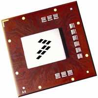
MPC8560PX833LB Freescale Semiconductor, MPC8560PX833LB Datasheet - Page 64

MPC8560PX833LB
Manufacturer Part Number
MPC8560PX833LB
Description
IC MPU POWERQUICC III 783-FCPBGA
Manufacturer
Freescale Semiconductor
Datasheet
1.MPC8560PX833LB.pdf
(104 pages)
Specifications of MPC8560PX833LB
Processor Type
MPC85xx PowerQUICC III 32-Bit
Speed
833MHz
Voltage
1.2V
Mounting Type
Surface Mount
Package / Case
783-FCPBGA
Family Name
MPC85XX
Device Core
PowerQUICC III
Device Core Size
32b
Frequency (max)
833MHz
Instruction Set Architecture
RISC
Supply Voltage 1 (typ)
1.2V
Operating Supply Voltage (max)
1.26V
Operating Supply Voltage (min)
1.14V
Operating Temp Range
0C to 105C
Operating Temperature Classification
Commercial
Mounting
Surface Mount
Pin Count
783
Package Type
FCBGA
For Use With
MPC8560ADS-BGA - BOARD APPLICATION DEV 8560
Lead Free Status / RoHS Status
Contains lead / RoHS non-compliant
Features
-
Lead Free Status / Rohs Status
Not Compliant
Available stocks
Company
Part Number
Manufacturer
Quantity
Price
Company:
Part Number:
MPC8560PX833LB
Manufacturer:
MOTOROLA
Quantity:
852
Company:
Part Number:
MPC8560PX833LB
Manufacturer:
Freescale Semiconductor
Quantity:
10 000
Part Number:
MPC8560PX833LB
Manufacturer:
NXP/恩智浦
Quantity:
20 000
RapidIO
The eye pattern for a data signal is generated by making a large number of recordings of the signal and
then overlaying the recordings. The number of recordings used to generate the eye shall be large enough
that further increasing the number of recordings used does not cause the resulting eye pattern to change
from one that complies with the RapidIO transmit mask to one that does not. Each data signal in the
interface shall be carrying random or pseudo-random data when the recordings are made. If
pseudo-random data is used, the length of the pseudo-random sequence (repeat length) shall be long
enough that increasing the length of the sequence does not cause the resulting eye pattern to change from
one that complies with the RapidIO transmit mask to one that does not comply with the mask. The data
carried by any given data signal in the interface may not be correlated with the data carried by any other
data signal in the interface. The zero-crossings of the clock associated with a data signal shall be used as
the timing reference for aligning the multiple recordings of the data signal when the recordings are
overlaid.
While the method used to make the recordings and overlay them to form the eye pattern is not specified,
the method used shall be demonstrably equivalent to the following method. The signal under test is
repeatedly recorded with a digital oscilloscope in infinite persistence mode. Each recording is triggered by
a zero-crossing of the clock associated with the data signal under test. Roughly half of the recordings are
triggered by positive-going clock zero-crossings and roughly half are triggered by negative-going clock
zero-crossings. Each recording is at least 1.9 UI in length (to ensure that at least one complete eye is
formed) and begins 0.5 UI before the trigger point (0.5 UI before the associated clock zero-crossing).
Depending on the length of the individual recordings used to generate the eye pattern, one or more
complete eyes will be formed. Regardless of the number of eyes, the eye whose center is immediately to
the right of the trigger point is the eye used for compliance testing.
An example of an eye pattern generated using the above method with recordings 3 UI in length is shown
in
to trigger the recordings. If skew was present, the eye pattern would be shifted to the left or right relative
to the oscilloscope trigger point.
64
.
Figure
45. In this example, there is no skew between the signal under test and the associated clock used
Trigger Point
Oscilloscope
(Recording)
MPC8560 Integrated Processor Hardware Specifications, Rev. 5
+
0
–
0.5 UI
Figure 45. Example Driver Output Eye Pattern
1.0 UI
Eye Used for
Compliance
Testing
1.0 UI
Eye Pattern
Freescale Semiconductor


