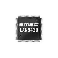
LAN9420I-NU SMSC, LAN9420I-NU Datasheet - Page 75

LAN9420I-NU
Manufacturer Part Number
LAN9420I-NU
Description
IC ETHERNET CTRLR SGL 128VTQFP
Manufacturer
SMSC
Type
Single Chip MAC and PHY Controllerr
Specifications of LAN9420I-NU
Controller Type
Ethernet Controller
Interface
PCI
Voltage - Supply
3 V ~ 3.6 V
Current - Supply
145mA
Operating Temperature
-40°C ~ 85°C
Mounting Type
Surface Mount
Package / Case
128-TQFP, 128-VQFP
Product
Ethernet Controllers
Number Of Transceivers
1
Standard Supported
802.3, 802.3u
Data Rate
10 MB, 100 MB
Supply Voltage (max)
3.6 V
Supply Voltage (min)
1.6 V
Maximum Operating Temperature
+ 85 C
Ethernet Connection Type
10/100 Base-T
Minimum Operating Temperature
- 40 C
Mounting Style
SMD/SMT
Lead Free Status / Rohs Status
Lead free / RoHS Compliant
Other names
638-1085
Available stocks
Company
Part Number
Manufacturer
Quantity
Price
Company:
Part Number:
LAN9420I-NU
Manufacturer:
Standard
Quantity:
368
Company:
Part Number:
LAN9420I-NU
Manufacturer:
SMSC
Quantity:
7 468
Company:
Part Number:
LAN9420I-NU
Manufacturer:
Microchip Technology
Quantity:
10 000
Single-Chip Ethernet Controller with HP Auto-MDIX Support and PCI Interface
Datasheet
SMSC LAN9420/LAN9420i
3.7.3
3.7.4
3.7.4.1
3.7.4.1.1
Device Clocking
LAN9420/LAN9420i requires a fixed-frequency 25MHz clock source. This is typically provided by
attaching a 25MHz crystal to the XI and XO pins. The clock can optionally be provided by driving the
XI input pin with a single-ended 25MHz clock source. If a single-ended source is selected, the clock
input must run continuously for normal device operation.
Internally, LAN9420/LAN9420i generates its required clocks with a phase-locked loop (PLL). The
LAN9420/LAN9420i reduces its power consumption in the D3 state by disabling its internal PLL and
derivative clocks. The 25MHz clock remains operational in all states where power is applied.
Please refer to
Power States
This section describes the operation of LAN9420/LAN9420i in each device power state (‘D’ states) as
well as the events required to cause state transitions. LAN9420/LAN9420i’s behavior is dependant on
the device’s VAUXDET pin (the device’s ability to detect wake events in D3
are discussed in the sections that follow.
Device power states and associated state transitions are illustrated in
Figure 3.28
G3 state as defined by the ACPI specification. In this state all power (+3.3V and 3.3Vaux) is off.
Some power state transitions may place the PHY in the General Power-Down state as noted in the
sections that follow. Please refer to
information on this mode of operation.
G3 State (Mechanical Off)
G3 is not a device power state, but is discussed here for illustrative purposes. In the G3 state all PCI
power is off. In this state all device context is lost.
POWER MANAGEMENT EVENTS IN G3
LAN9420/LAN9420i does not detect power management events in the G3 state.
includes the system’s mechanical off (G3) power state for illustrative purposes. This is the
D3
D0
T3
Section 5.9, "Clock Circuit," on page 166
Figure 3.28 LAN9420/LAN9420i Device Power States
HOT
A
T11
T7
T2
T4
DATASHEET
Section 3.6.8.1, "General Power-Down," on page 72
75
D3
T9
D0
COLD
T10
U
for more information on clock requirements.
T6
G3
Figure 3.28
COLD
Revision 1.4 (12-17-08)
). Specific behaviors
T12
below. Note that
Vaux Off
for more


