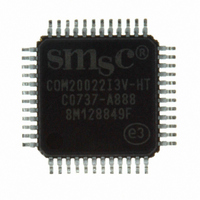
COM20022I3V-HT SMSC, COM20022I3V-HT Datasheet - Page 44

COM20022I3V-HT
Manufacturer Part Number
COM20022I3V-HT
Description
IC CTRLR ARCNET 2KX8 RAM 48-TQFP
Manufacturer
SMSC
Series
ARCNETr
Datasheet
1.COM20022I3V-HT.pdf
(82 pages)
Specifications of COM20022I3V-HT
Controller Type
ARCNET Controller
Interface
Differential
Voltage - Supply
4.5 V ~ 5.5 V
Current - Supply
65mA
Operating Temperature
-40°C ~ 85°C
Mounting Type
Surface Mount
Package / Case
48-TQFP, 48-VQFP
Lead Free Status / RoHS Status
Lead free / RoHS Compliant
Other names
638-1004
Available stocks
Company
Part Number
Manufacturer
Quantity
Price
Company:
Part Number:
COM20022I3V-HT
Manufacturer:
Standard
Quantity:
2 784
Company:
Part Number:
COM20022I3V-HT
Manufacturer:
AD
Quantity:
7 439
Company:
Part Number:
COM20022I3V-HT
Manufacturer:
Microchip Technology
Quantity:
10 000
Part Number:
COM20022I3V-HT
Manufacturer:
SMSC
Quantity:
20 000
Revision 09-27-07
BIT
5,4
7
6
3
2
Read Bus Timing
Select
Reserved
Clock Multiplier
Enhanced Functions
No Synchronous
BIT NAME
RBUSTMG
CKUP1, 0
EF
NOSYNC
SYMBOL
Table 6.11 - Setup 2 Register
DATASHEET
This bit is used to Disable/Enable the High Speed CPU Read
function for High Speed CPU bus support. RBUSTMG=0: Disable
(Default), RBUSTMG=1: Enable. That is, if BUSTMG (pin 26) = 1
and RBUSTMG = 1, High Speed CPU Read operations are
enabled. It does not influence write operation. High speed CPU
Read operation is only for non-multiplexed bus.
This bit is undefined.
Higher frequency clocks are generated from the 20 MHz crystal
through the selection of these two bits as shown. This clock
multiplier is powered-down on default. After changing the CKUP1
and CKUP0 bits, the ARCNET core operation is stopped and the
internal PLL in the clock multiplier is awakened and it starts to
generate the 40 MHz. The lock out time of the internal PLL is 8 μ Sec
typically. After 1 mS it is necessary to write command data '18H' to
command register for re-starting the ARCNET core operation. EF
bit must be ‘1’ if the data rate is over 5Mbps.
CAUTION: Changing the CKUP1 and CKUP0 bits must be one
time or less after releasing a hardware reset.
Note: After changing the CKUP1 or CKUP0 bits, it is necessary to
These initializing steps are shown below.
1.
2.
3.
4.
5.
This bit is used to enable the new enhanced functions in the
COM20022I. EF = 0: Disable (Default), EF = 1: Enable. If EF = 0,
the timing and function is the same as in the COM20020, Revision
B. See appendix “A”. EF bit must be ‘1’ if the data rate is over
5Mbps.
EF bit should be ‘1’ for new design customers.
EF bit should be ‘0’ for replacement customers.
This bit is used to enable the SYNC command during initialization.
NOSYNC= 0, Enable (Default) The line must be idle for the RAM
initialization sequence to be written. NOSYNC= 1, Disable:) The line
does not have to be idle for the RAM initialization sequence to be
written. See appendix “A”.
CKUP1
Hardware reset (Power ON)
Change CKUP[1, 0] bit
Wait 1mSec (wait until stable oscillation)
Write command '18H' (start internal operation)
Start initializing routine (Execute existing software)
0
0
1
1
Page 44
write a command data '18H' to the command register.
Because after changing the CKUP [1, 0] bits, the internal
operation is stopped temporarily. The writing of the
command is to start the operation.
10 Mbps ARCNET (ANSI 878.1) Controller with 2Kx8 On-Chip RAM
CKUP0
0
1
0
1
DESCRIPTION
20 MHz (Up to 2.5Mbps) Default
40 MHz (Up to 5Mbps)
Reserved
80 MHz (Only 10Mbps)
Clock Frequency (Data Rate)
SMSC COM20022I
Datasheet


