DP83848TSQ/NOPB National Semiconductor, DP83848TSQ/NOPB Datasheet - Page 10
DP83848TSQ/NOPB
Manufacturer Part Number
DP83848TSQ/NOPB
Description
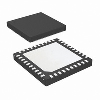
IC TXRX ETHERNET PHYTER 40-LLP
Manufacturer
National Semiconductor
Type
Transceiverr
Specifications of DP83848TSQ/NOPB
Number Of Drivers/receivers
1/1
Protocol
Ethernet
Voltage - Supply
3 V ~ 3.6 V
Mounting Type
Surface Mount
Package / Case
40-LLP
Data Rate
100Mbps
Supply Voltage Range
3V To 3.6V
Logic Case Style
LLP
No. Of Pins
40
Operating Temperature Range
-40°C To +85°C
Msl
MSL 2 - 1 Year
Filter Terminals
SMD
Rohs Compliant
Yes
Data Rate Max
10Mbps
Driver Case Style
LLP
For Use With
DP83848T-MAU-EK - BOARD EVALUATION DP83848T
Lead Free Status / RoHS Status
Lead free / RoHS Compliant
Other names
DP83848TSQTR
Available stocks
Company
Part Number
Manufacturer
Quantity
Price
Company:

Part Number:
DP83848TSQ/NOPB
Manufacturer:
TI
Quantity:
2 000
Company:
Part Number:
DP83848TSQ/NOPB
Manufacturer:
LT
Quantity:
807


www.national.com
1.3 Clock Interface
RX_ER
RXD_0
RXD_1
RXD_2
RXD_3
CRS/CRS_DV
COL
X1
X2
Signal Name
Signal Name
S, O, PU
S, O, PD
S, O, PU
S, O, PU
Type
Type
O
I
Pin #
Pin #
34
36
37
38
39
33
35
28
27
MII RECEIVE ERROR: Asserted high synchronously to RX_CLK
to indicate that an invalid symbol has been detected within a re-
ceived packet in 100 Mb/s mode.
RMII RECEIVE ERROR: Assert high synchronously to X1 when-
ever it detects a media error and RX_DV is asserted in 100 Mb/s
mode.
This pin is not required to be used by a MAC, in either MII or RMII
mode, since the Phy is required to corrupt data on a receive error.
MII RECEIVE DATA: Nibble wide receive data signals driven syn-
chronously to the RX_CLK, 25 MHz for 100 Mb/s mode, 2.5 MHz
for 10 Mb/s mode). RXD[3:0] signals contain valid data when
RX_DV is asserted.
RMII RECEIVE DATA: 2-bits receive data signals, RXD[1:0], driv-
en synchronously to the X1 clock, 50 MHz.
MII CARRIER SENSE: Asserted high to indicate the receive me-
dium is non-idle.
RMII CARRIER SENSE/RECEIVE DATA VALID: This signal
combines the RMII Carrier and Receive Data Valid indications.
For a detailed description of this signal, see the RMII Specifica-
tion.
MII COLLISION DETECT: Asserted high to indicate detection of
a collision condition (simultaneous transmit and receive activity)
in 10 Mb/s and 100 Mb/s Half Duplex Modes.
While in 10BASE-T Half Duplex mode with heartbeat enabled this
pin is also asserted for a duration of approximately 1 s at the end
of transmission to indicate heartbeat (SQE test).
In Full Duplex Mode, for 10 Mb/s or 100 Mb/s operation, this sig-
nal is always logic 0. There is no heartbeat function during 10
Mb/s full duplex operation.
RMII COLLISION DETECT: Per the RMII Specification, no COL
signal is required. The MAC will recover CRS from the CRS_DV
signal and use that along with its TX_EN signal to determine col-
lision.
CRYSTAL/OSCILLATOR INPUT: This pin is the primary clock
reference input for the DP83848T and must be connected to a 25
MHz 0.005% (+50 ppm) clock source. The DP83848T supports
either an external crystal resonator connected across pins X1 and
X2, or an external CMOS-level oscillator source connected to pin
X1 only.
RMII REFERENCE CLOCK: This pin is the primary clock refer-
ence input for the RMII mode and must be connected to a 50 MHz
0.005% (+50 ppm) CMOS-level oscillator source.
CRYSTAL OUTPUT: This pin is the primary clock reference out-
put to connect to an external 25 MHz crystal resonator device.
This pin must be left unconnected if an external CMOS oscillator
clock source is used.
10
Description
Description
Related parts for DP83848TSQ/NOPB
Image
Part Number
Description
Manufacturer
Datasheet
Request
R

Part Number:
Description:
BOARD EVALUATION DP83848T
Manufacturer:
National Semiconductor
Datasheet:
Part Number:
Description:
National Semiconductor [8-Bit D/A Converter]
Manufacturer:
National Semiconductor
Datasheet:
Part Number:
Description:
National Semiconductor [Media Coprocessor]
Manufacturer:
National Semiconductor
Datasheet:
Part Number:
Description:
Digitally Controlled Tone and Volume Circuit with Stereo Audio Power Amplifier, Microphone Preamp Stage and National 3D Sound
Manufacturer:
National Semiconductor
Datasheet:
Part Number:
Description:
Digitally Controlled Tone and Volume Circuit with Stereo Audio Power Amplifier, Microphone Preamp Stage and National 3D Sound
Manufacturer:
National Semiconductor
Datasheet:
Part Number:
Description:
AC97 Rev 2 Codec with Sample Rate Conversion and National 3D Sound
Manufacturer:
National Semiconductor
Part Number:
Description:
Manufacturer:
National Semiconductor
Datasheet:
Part Number:
Description:
Manufacturer:
National Semiconductor
Datasheet:
Part Number:
Description:
General Purpose, Low Voltage, Low Power, Rail-to-Rail Output Operational Amplifiers
Manufacturer:
National Semiconductor
Datasheet:
Part Number:
Description:
8-bit 20 MSPS flash A/D converter.
Manufacturer:
National Semiconductor
Datasheet:
Part Number:
Description:
Low Noise Quad Operational Amplifier
Manufacturer:
National Semiconductor
Datasheet:
Part Number:
Description:
Quad Differential Line Receivers
Manufacturer:
National Semiconductor
Datasheet:
Part Number:
Description:
Quad High Speed Trapezoidal? Bus Transceiver
Manufacturer:
National Semiconductor
Datasheet:
Part Number:
Description:
Dual Line Receiver
Manufacturer:
National Semiconductor
Datasheet: