DP83848TSQ/NOPB National Semiconductor, DP83848TSQ/NOPB Datasheet - Page 11
DP83848TSQ/NOPB
Manufacturer Part Number
DP83848TSQ/NOPB
Description
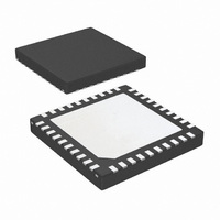
IC TXRX ETHERNET PHYTER 40-LLP
Manufacturer
National Semiconductor
Type
Transceiverr
Specifications of DP83848TSQ/NOPB
Number Of Drivers/receivers
1/1
Protocol
Ethernet
Voltage - Supply
3 V ~ 3.6 V
Mounting Type
Surface Mount
Package / Case
40-LLP
Data Rate
100Mbps
Supply Voltage Range
3V To 3.6V
Logic Case Style
LLP
No. Of Pins
40
Operating Temperature Range
-40°C To +85°C
Msl
MSL 2 - 1 Year
Filter Terminals
SMD
Rohs Compliant
Yes
Data Rate Max
10Mbps
Driver Case Style
LLP
For Use With
DP83848T-MAU-EK - BOARD EVALUATION DP83848T
Lead Free Status / RoHS Status
Lead free / RoHS Compliant
Other names
DP83848TSQTR
Available stocks
Company
Part Number
Manufacturer
Quantity
Price
Company:

Part Number:
DP83848TSQ/NOPB
Manufacturer:
TI
Quantity:
2 000
Company:
Part Number:
DP83848TSQ/NOPB
Manufacturer:
LT
Quantity:
807


1.4 LED Interface
See Table 3 for LED Mode Selection.
1.5 Reset
1.6 Strap Options
DP83848T uses many functional pins as strap options. The
values of these pins are sampled during reset and used to
strap the device into specific modes of operation. The strap
option pin assignments are defined below. The functional
pin name is indicated in parentheses.
25MHz_OUT
LED_LINK
RESET_N
PHYAD0 (COL)
PHYAD1 (RXD_0)
PHYAD2 (RXD_1)
PHYAD3 (RXD_2)
PHYAD4 (RXD_3)
Signal Name
Signal Name
Signal Name
Signal Name
S, O, PU
S, O, PU
S, O, PD
Type
Type
Type
Type
I, PU
O
Pin #
Pin #
Pin #
Pin #
21
22
23
35
36
37
38
39
25 MHz CLOCK OUTPUT:
This pin provides a 25 MHz clock output to the system. This al-
lows other devices to use the reference clock from the DP83848T
without requiring additional clock sources.
RMII Mode: This pin provides a 50 MHz clock output to the sys-
tem. For RMII mode, it is not recommended that the system clock
out be used as the reference clock to the MAC without first verify-
ing the interface timing. See AN-1405 for more details.
LINK LED: In Mode 1, this pin indicates the status of the LINK.
The LED will be ON when Link is good.
LINK/ACT LED: In Mode 2, this pin indicates transmit and receive
activity in addition to the status of the Link. The LED will be ON
when Link is good. It will blink when the transmitter or receiver is
active.
RESET: Active Low input that initializes or re-initializes the
DP83848T. Asserting this pin low for at least 1 s will force a reset
process to occur. All internal registers will re-initialize to their de-
fault states as specified for each bit in the Register Block section.
All strap options are re-initialized as well.
PHY ADDRESS [4:0]: The DP83848T provides five PHY address
pins, the state of which are latched into the PHYCTRL register at
system Hardware-Reset.
The DP83848T supports PHY Address strapping values 0
(<00000>) through 31 (<11111>). A PHY Address of 0 puts the
part into the MII Isolate Mode. The MII isolate mode must be se-
lected by strapping Phy Address 0; changing to Address 0 by reg-
ister write will not put the Phy in the MII isolate mode. Please refer
to section 2.3 for additional information.
PHYAD0 pin has weak internal pull-up resistor.
PHYAD[4:1] pins have weak internal pull-down resistors.
11
A 2.2 k resistor should be used for pull-down or pull-up to
change the default strap option. If the default option is
required, then there is no need for external pull-up or pull
down resistors. Since these pins may have alternate func-
tions after reset is deasserted, they should not be con-
nected directly to VCC or GND.
Description
Description
Description
Description
www.national.com
Related parts for DP83848TSQ/NOPB
Image
Part Number
Description
Manufacturer
Datasheet
Request
R

Part Number:
Description:
BOARD EVALUATION DP83848T
Manufacturer:
National Semiconductor
Datasheet:
Part Number:
Description:
National Semiconductor [8-Bit D/A Converter]
Manufacturer:
National Semiconductor
Datasheet:
Part Number:
Description:
National Semiconductor [Media Coprocessor]
Manufacturer:
National Semiconductor
Datasheet:
Part Number:
Description:
Digitally Controlled Tone and Volume Circuit with Stereo Audio Power Amplifier, Microphone Preamp Stage and National 3D Sound
Manufacturer:
National Semiconductor
Datasheet:
Part Number:
Description:
Digitally Controlled Tone and Volume Circuit with Stereo Audio Power Amplifier, Microphone Preamp Stage and National 3D Sound
Manufacturer:
National Semiconductor
Datasheet:
Part Number:
Description:
AC97 Rev 2 Codec with Sample Rate Conversion and National 3D Sound
Manufacturer:
National Semiconductor
Part Number:
Description:
Manufacturer:
National Semiconductor
Datasheet:
Part Number:
Description:
Manufacturer:
National Semiconductor
Datasheet:
Part Number:
Description:
General Purpose, Low Voltage, Low Power, Rail-to-Rail Output Operational Amplifiers
Manufacturer:
National Semiconductor
Datasheet:
Part Number:
Description:
8-bit 20 MSPS flash A/D converter.
Manufacturer:
National Semiconductor
Datasheet:
Part Number:
Description:
Low Noise Quad Operational Amplifier
Manufacturer:
National Semiconductor
Datasheet:
Part Number:
Description:
Quad Differential Line Receivers
Manufacturer:
National Semiconductor
Datasheet:
Part Number:
Description:
Quad High Speed Trapezoidal? Bus Transceiver
Manufacturer:
National Semiconductor
Datasheet:
Part Number:
Description:
Dual Line Receiver
Manufacturer:
National Semiconductor
Datasheet: