DP83848TSQ/NOPB National Semiconductor, DP83848TSQ/NOPB Datasheet - Page 9
DP83848TSQ/NOPB
Manufacturer Part Number
DP83848TSQ/NOPB
Description
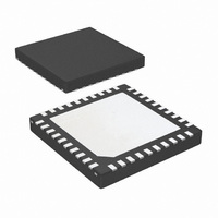
IC TXRX ETHERNET PHYTER 40-LLP
Manufacturer
National Semiconductor
Type
Transceiverr
Specifications of DP83848TSQ/NOPB
Number Of Drivers/receivers
1/1
Protocol
Ethernet
Voltage - Supply
3 V ~ 3.6 V
Mounting Type
Surface Mount
Package / Case
40-LLP
Data Rate
100Mbps
Supply Voltage Range
3V To 3.6V
Logic Case Style
LLP
No. Of Pins
40
Operating Temperature Range
-40°C To +85°C
Msl
MSL 2 - 1 Year
Filter Terminals
SMD
Rohs Compliant
Yes
Data Rate Max
10Mbps
Driver Case Style
LLP
For Use With
DP83848T-MAU-EK - BOARD EVALUATION DP83848T
Lead Free Status / RoHS Status
Lead free / RoHS Compliant
Other names
DP83848TSQTR
Available stocks
Company
Part Number
Manufacturer
Quantity
Price
Company:

Part Number:
DP83848TSQ/NOPB
Manufacturer:
TI
Quantity:
2 000
Company:
Part Number:
DP83848TSQ/NOPB
Manufacturer:
LT
Quantity:
807


1.0 Pin Descriptions
The DP83848T pins are classified into the following inter-
face categories (each interface is described in the sections
that follow):
— Serial Management Interface
— MAC Data Interface
— Clock Interface
— LED Interface
— Reset
— Strap Options
— 10/100 Mb/s PMD Interface
— Special Connect Pins
— Power and Ground pins
1.1 Serial Management Interface
1.2 MAC Data Interface
MDC
MDIO
TX_CLK
TX_EN
TXD_0
TXD_1
TXD_2
TXD_3
RX_CLK
RX_DV
Signal Name
Signal Name
O, PD
Type
Type
I, PD
I, PD
I/O
O
O
I
I
Pin #
Pin #
25
24
31
32
2
3
4
5
6
7
MANAGEMENT DATA CLOCK: Synchronous clock to the MDIO
management data input/output serial interface which may be
asynchronous to transmit and receive clocks. The maximum clock
rate is 25 MHz with no minimum clock rate.
MANAGEMENT DATA I/O: Bi-directional management instruc-
tion/data signal that may be sourced by the station management
entity or the PHY. This pin requires a 1.5 k
MII TRANSMIT CLOCK: 25 MHz Transmit clock output in 100
Mb/s mode or 2.5 MHz in 10 Mb/s mode derived from the 25 MHz
reference clock.
Unused in RMII mode. The device uses the X1 reference clock in-
put as the 50 MHz reference for both transmit and receive.
MII TRANSMIT ENABLE: Active high input indicates the pres-
ence of valid data inputs on TXD[3:0].
RMII TRANSMIT ENABLE: Active high input indicates the pres-
ence of valid data on TXD[1:0].
MII TRANSMIT DATA: Transmit data MII input pins, TXD[3:0],
that accept data synchronous to the TX_CLK (2.5 MHz in 10 Mb/s
mode or 25 MHz in 100 Mb/s mode).
RMII TRANSMIT DATA: Transmit data RMII input pins, TXD[1:0],
that accept data synchronous to the 50 MHz reference clock.
MII RECEIVE CLOCK: Provides the 25 MHz recovered receive
clock for 100 Mb/s mode and 2.5 MHz for 10 Mb/s mode.
Unused in RMII mode. The device uses the X1 reference clock in-
put as the 50 MHz reference for both transmit and receive.
MII RECEIVE DATA VALID: Asserted high to indicate that valid
data is present on the corresponding RXD[3:0].
RMII Synchronous Receive Data Valid: This signal provides the
RMII Receive Data Valid indication independent of Carrier Sense.
9
Note: Strapping pin option. Please see Section 1.61.6 for
strap definitions.
All DP83848T signal pins are I/O cells regardless of the
particular use. The definitions below define the functionality
of the I/O cells for each pin.
Type: I
Type: O
Type: I/O
Type: PD,PU Internal Pulldown/Pullup
Type: S
Input
Output
Input/Output
Strapping Pin (All strap pins have weak in-
ternal pull-ups or pull-downs. If the default
strap value is needed to be changed then an
external 2.2 k
Please see Section 1.6 1.6 for details.)
Description
Description
resistor should be used.
pullup resistor.
www.national.com
Related parts for DP83848TSQ/NOPB
Image
Part Number
Description
Manufacturer
Datasheet
Request
R

Part Number:
Description:
BOARD EVALUATION DP83848T
Manufacturer:
National Semiconductor
Datasheet:
Part Number:
Description:
National Semiconductor [8-Bit D/A Converter]
Manufacturer:
National Semiconductor
Datasheet:
Part Number:
Description:
National Semiconductor [Media Coprocessor]
Manufacturer:
National Semiconductor
Datasheet:
Part Number:
Description:
Digitally Controlled Tone and Volume Circuit with Stereo Audio Power Amplifier, Microphone Preamp Stage and National 3D Sound
Manufacturer:
National Semiconductor
Datasheet:
Part Number:
Description:
Digitally Controlled Tone and Volume Circuit with Stereo Audio Power Amplifier, Microphone Preamp Stage and National 3D Sound
Manufacturer:
National Semiconductor
Datasheet:
Part Number:
Description:
AC97 Rev 2 Codec with Sample Rate Conversion and National 3D Sound
Manufacturer:
National Semiconductor
Part Number:
Description:
Manufacturer:
National Semiconductor
Datasheet:
Part Number:
Description:
Manufacturer:
National Semiconductor
Datasheet:
Part Number:
Description:
General Purpose, Low Voltage, Low Power, Rail-to-Rail Output Operational Amplifiers
Manufacturer:
National Semiconductor
Datasheet:
Part Number:
Description:
8-bit 20 MSPS flash A/D converter.
Manufacturer:
National Semiconductor
Datasheet:
Part Number:
Description:
Low Noise Quad Operational Amplifier
Manufacturer:
National Semiconductor
Datasheet:
Part Number:
Description:
Quad Differential Line Receivers
Manufacturer:
National Semiconductor
Datasheet:
Part Number:
Description:
Quad High Speed Trapezoidal? Bus Transceiver
Manufacturer:
National Semiconductor
Datasheet:
Part Number:
Description:
Dual Line Receiver
Manufacturer:
National Semiconductor
Datasheet: