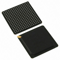
PI7C9X130DNDE Pericom Semiconductor, PI7C9X130DNDE Datasheet - Page 57

PI7C9X130DNDE
Manufacturer Part Number
PI7C9X130DNDE
Description
IC PCIE-PCIX BRIDGE 1PORT 256BGA
Manufacturer
Pericom Semiconductor
Specifications of PI7C9X130DNDE
Applications
PCI-to-PCI Bridge
Interface
SMBus (2-Wire/I²C)
Voltage - Supply
1.8V, 3.3V
Package / Case
256-PBGA
Mounting Type
Surface Mount
Operating Temperature (min)
-40C
Operating Temperature Classification
Industrial
Operating Temperature (max)
85C
Package Type
BGA
Rad Hardened
No
Lead Free Status / RoHS Status
Lead free / RoHS Compliant
Available stocks
Company
Part Number
Manufacturer
Quantity
Price
Company:
Part Number:
PI7C9X130DNDE
Manufacturer:
Pericom
Quantity:
135
Company:
Part Number:
PI7C9X130DNDE
Manufacturer:
NSC
Quantity:
70
7.4.48 PCI-X BRIDGE STATUS REGISTER – OFFSET 84h
PERICOM SEMICONDUCTOR - Confidential
Bit
19
20
21
24:22
31:25
Bit
2:0
7:3
Function
Unexpected Split
Completion
Split Completion
Overrun
Split Request
Delayed
Secondary Clock
Frequency
Reserved
Function
Function Number
Device Number
Type
Type
RWC
RWC
RWC
RO
RO
RO
RO
Page 57 of 165
Description
secondary bus because the requester did not accept the split completion
transaction
Reset to 0
This bit is set to 0 in forward bridge mode or is read-write in reverse bridge
mode
When this bit is set to 1, an unexpected split completion has been received with
the requester ID equaled to the secondary bus number, device number, and
function number at the PI7X9X130 secondary bus interface
Reset to 0
When this bit is set to 1, a split completion has been terminated by PI7C9X130
with either a retry or disconnect at the next ADB due to the buffer full
condition
Reset to 0
When this bit is set to 1, a split request is delayed because PI7C9X130 is not
able to forward the split request transaction to its secondary bus due to
insufficient room within the limit specified in the split transaction commitment
limit field of the downstream split transaction control register
Reset to 0
These bits are only meaningful in forward bridge mode. In reverse bridge
mode, all three bits are set to zero.
000: Conventional PCI mode (minimum clock period not applicable)
001: 66MHz (minimum clock period is 15ns)
010: 100 to 133MHz (minimum clock period is 7.5ns)
011: Reserved
1xx: Reserved
Reset to 000
0000000
Description
Function number (AD [10:8] of a type 0 configuration transaction)
Reset to 000
Device number (AD [15:11] of a type 0 configuration transaction) is assigned
to the PI7C9X130 by the connection of system hardware. Each time the
PI7C9X130 is addressed by a configuration write transaction, the bridge
updates this register with the contents of AD [15:11] of the address phase of the
configuration transaction, regardless of which register in the PI7C9X130 is
addressed by the transaction. The PI7C9X130 is addressed by a configuration
write transaction if all of the following are true:
Reset to 11111
The transaction uses a configuration write command
IDSEL is asserted during the address phase
AD [1:0] are 00 (type o configuration transaction)
AD [10:8] of the configuration address contain the appropriate function
number
PCI EXPRESS TO PCI-X BRIDGE
Mar 2010 - Rev 2.0
PI7C9X130


