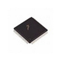
DSPB56364FU100 Freescale Semiconductor, DSPB56364FU100 Datasheet - Page 18

DSPB56364FU100
Manufacturer Part Number
DSPB56364FU100
Description
Manufacturer
Freescale Semiconductor
Datasheet
1.DSPB56364FU100.pdf
(148 pages)
Specifications of DSPB56364FU100
Device Core Size
24b
Format
Fixed Point
Clock Freq (max)
100MHz
Mips
100
Device Input Clock Speed
100MHz
Ram Size
9KB
Program Memory Size
24KB
Operating Supply Voltage (typ)
3.3V
Operating Supply Voltage (min)
3.14V
Operating Supply Voltage (max)
3.46V
Operating Temp Range
-40C to 105C
Operating Temperature Classification
Industrial
Mounting
Surface Mount
Pin Count
100
Package Type
LQFP
Lead Free Status / Rohs Status
Not Compliant
Available stocks
Company
Part Number
Manufacturer
Quantity
Price
Company:
Part Number:
DSPB56364FU100
Manufacturer:
MOTOLOLA
Quantity:
319
Part Number:
DSPB56364FU100
Manufacturer:
MOTOROLA/摩托罗拉
Quantity:
20 000
Part Number:
DSPB56364FU100-4J2
Manufacturer:
FREESCALE
Quantity:
20 000
Thermal Characteristics
3.3
1
2
3-2
1
2
3
Junction-to-ambient thermal resistance
Junction-to-case thermal resistance
Thermal characterization parameter
Supply Voltage
All input voltages excluding “5 V tolerant” inputs
All “5 V tolerant” input voltages
Current drain per pin excluding V
Operating temperature range
Storage temperature
Junction-to-ambient thermal resistance is based on measurements on a horizontal single-sided printed circuit board per SEMI
G38-87 in natural convection. (SEMI is Semiconductor Equipment and Materials International, 805 East Middlefield Rd.,
Mountain View, CA 94043, (415) 964-5111.)
Measurements were done with parts mounted on thermal test boards conforming to specification EIA/JESD51-3.
Junction-to-case thermal resistance is based on measurements using a cold plate per SEMI G30-88, with the exception that
the cold plate temperature is used for the case temperature.
GND = 0 V, V
Absolute maximum ratings are stress ratings only, and functional operation at the maximum is not guaranteed. Stress beyond
the maximum rating may affect device reliability or cause permanent damage to the device.
CAUTION: All “5 V Tolerant” input voltages must not be more than 3.95 V greater than the supply voltage; this restriction
applies to “power on”, as well as during normal operation. In any case, the input voltages cannot be more than 5.75 V. “5 V
Tolerant” inputs are inputs that tolerate 5 V.
Thermal Characteristics
CC
= 3.3 V ± 0.16 V, T
Characteristic
Rating
3
1
CC
2
and GND
J
1
= –0°C to +105°C, C
Table 3-2 Thermal Characteristics
DSP56364 Technical Data, Rev. 4.1
Table 3-1 Maximum Ratings
3
L
= 50 pF
Symbol
T
V
V
V
STG
T
IN5
CC
I
IN
J
R
R
Symbol
θJC
θJA
Ψ
or θ
or θ
JT
JA
JC
GND
GND -0.3 to V
−
−
−
-40 to +105
0.3 to V
0.3 to +4.0
55 to +125
Value
TQFP Value
10
49.87
9.26
1, 2
2.0
CC
CC
+ 0.3
+ 3.95
Freescale Semiconductor
°
°
°
Unit
C/W
C/W
C/W
Unit
mA
°
°
V
V
V
C
C


