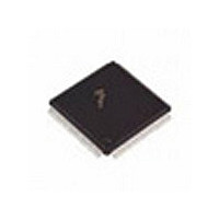
DSPB56364FU100 Freescale Semiconductor, DSPB56364FU100 Datasheet - Page 8

DSPB56364FU100
Manufacturer Part Number
DSPB56364FU100
Description
Manufacturer
Freescale Semiconductor
Datasheet
1.DSPB56364FU100.pdf
(148 pages)
Specifications of DSPB56364FU100
Device Core Size
24b
Format
Fixed Point
Clock Freq (max)
100MHz
Mips
100
Device Input Clock Speed
100MHz
Ram Size
9KB
Program Memory Size
24KB
Operating Supply Voltage (typ)
3.3V
Operating Supply Voltage (min)
3.14V
Operating Supply Voltage (max)
3.46V
Operating Temp Range
-40C to 105C
Operating Temperature Classification
Industrial
Mounting
Surface Mount
Pin Count
100
Package Type
LQFP
Lead Free Status / Rohs Status
Not Compliant
Available stocks
Company
Part Number
Manufacturer
Quantity
Price
Company:
Part Number:
DSPB56364FU100
Manufacturer:
MOTOLOLA
Quantity:
319
Part Number:
DSPB56364FU100
Manufacturer:
MOTOROLA/摩托罗拉
Quantity:
20 000
Part Number:
DSPB56364FU100-4J2
Manufacturer:
FREESCALE
Quantity:
20 000
Clock and PLL
2.4
2.5
When the DSP56364 enters a low-power standby mode (stop or wait), it tri-states the relevant port A
signals: D0–D7, AA0, AA1, RD, WR, CAS.
2.5.1
2-4
Signal Name
Signal Name
Ground Name
PINIT/NMI
A0–A17
EXTAL
GND
PCAP
GND
C
S
Clock and PLL
External Memory Expansion Port (Port A)
(3)
(1)
External Address Bus
Type
Input
Input
Input
Bus Control Ground—GND
be tied externally to all other chip ground connections. The user must provide adequate external decoupling
capacitors. There is one GND
SHI and ESAI —GND
to all other chip ground connections. The user must provide adequate external decoupling capacitors.
There are three GND
Output
Type
State During
Reset
Input
Input
Input
Keeper active Address Bus—A0–A17 are active-high outputs that specify the address for
State During
Reset
Table 2-5 External Address Bus Signals
S
S
External Clock Input—An external clock source must be connected to EXTAL in
order to supply the clock to the internal clock generator and PLL.
PLL Capacitor—PCAP is an input connecting an off-chip capacitor to the PLL filter.
Connect one capacitor terminal to PCAP and the other terminal to V
If the PLL is not used, PCAP may be tied to V
PLL Initial/Nonmaskable Interrupt—During assertion of RESET, the value of
PINIT/NMI is written into the PLL Enable (PEN) bit of the PLL control register,
determining whether the PLL is enabled or disabled. After RESET de assertion and
during normal instruction processing, the PINIT/NMI Schmitt-trigger input is a
negative-edge-triggered nonmaskable interrupt (NMI) request internally
synchronized to internal system clock.
This input is 5 V tolerant.
connections.
is an isolated ground for the SHI and ESAI. This connection must be tied externally
Table 2-4 Clock and PLL Signals
Table 2-3 Grounds (continued)
DSP56364 Technical Data, Rev. 4.1
external program and data memory accesses. Otherwise, the signals are kept
to their previous values by internal weak keepers. To minimize power
dissipation, A0–A17 do not change state when external memory spaces are not
being accessed.
C
C
is an isolated ground for the bus control I/O drivers. This connection must
connections.
Description
Signal Description
Signal Description
CC
, GND, or left floating.
Freescale Semiconductor
CCP
.


