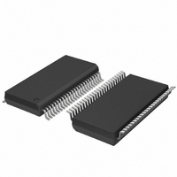
SC28L201A1DGG,118 NXP Semiconductors, SC28L201A1DGG,118 Datasheet - Page 66

SC28L201A1DGG,118
Manufacturer Part Number
SC28L201A1DGG,118
Description
IC UART W/FIFO 48-TSSOP
Manufacturer
NXP Semiconductors
Series
IMPACTr
Datasheet
1.SC28L201A1DGG118.pdf
(110 pages)
Specifications of SC28L201A1DGG,118
Features
False-start Bit Detection
Number Of Channels
2, DUART
Fifo's
256 Byte
Voltage - Supply
3.3V, 5V
With Parallel Port
Yes
With Auto Flow Control
Yes
With False Start Bit Detection
Yes
With Modem Control
Yes
With Cmos
Yes
Mounting Type
Surface Mount
Package / Case
48-TSSOP
Lead Free Status / RoHS Status
Lead free / RoHS Compliant
Other names
935277824118
SC28L201A1DGG-T
SC28L201A1DGG-T
SC28L201A1DGG-T
SC28L201A1DGG-T
Philips Semiconductors
9397 750 13138
Product data sheet
8.4.4 Counter Timer Value Registers, Upper 0 and Upper 1 (CTVU0, CTVU1)
8.4.5 Counter Timer Value Registers, Lower 0 and Lower 1 (CTVL0, CTVL1)
8.4.6 Programmable BRG Clock Source, 0 and 1 (PBRGCS)
Reading this register gives the value of the upper 8 bits of the Counter/Timer.
Table 41:
Reading this register gives the value of the lower 8 bits of the Counter/Timer.
Table 42:
Remark: The Counter/Timer should be stopped before reading. Usually the clock of the
Counter/Timer is not synchronized with the read of the C/T. It is therefore possible to
capture changing data during the read. Depending on the clock speed with respect to the
read cycle, this could be made worse or completely eliminated. If the ‘Stop counter’
command is issued and following that the C/T is read, there will be no uncertainty to its
value. If it is necessary to read the C/T ‘on the fly’, then reading it twice and comparing the
values will correct the problem. The double read will not be effective if the counter timer
clock is faster than a read cycle.
Start/Stop control and Clock Select register for the two BRG counters. The clock selection
is for the input to the counters. It is that clock divided by the number represented by the
PBRGPU and PBRGPL then will be used as the 16 clock for the receivers and
transmitters. When the BRG timer Clock is selected for the receiver(s) or transmitter(s) the
receivers and transmitters will consider it as a 16 clock and further divide it by 16. In
other words, the receivers and transmitters will always be in the 16 mode of operation
when the internal BRG timer is selected for their clock.
Table 43:
Bit
7:0
Bit
7:0
Bit
7
6:4
Symbol
Symbol
Symbol
CTVU0, CTVU1 - Counter Timer Value registers, Upper 0 and Upper 1
(address 0x16, 0x1E) bit description
CTVL0, CTVL1 - Counter Timer Value registers, Lower 0 and Lower 1
(address 0x17, 0x1F) bit description
PBRGCS - Programmable BRG Clock Source 0 and 1 register (address 0x33) bit
description
Description
8 MSBs of the Counter/Timer preset value
Description
8 LSBs of the Counter/Timer preset value
Description
PBRG 1 register control
PBRG 1 clock selection
Rev. 01 — 31 October 2005
0 = resets PBRG 1 and holds it stopped
1 = allows PBRG 1 to run
000 = SCLK
001 = SCLK/2
010 = SCLK/6
011 = SCLK/32
100 = SCLK/64
101 = SCLK/128
110 = I/O4A
111 = reserved
3.3 V, 5 V UART, 3.125 Mbit/s, with 256-byte FIFO
© Koninklijke Philips Electronics N.V. 2005. All rights reserved.
SC28L201
66 of 110


