SC28L201A1DGG,118 NXP Semiconductors, SC28L201A1DGG,118 Datasheet - Page 9
SC28L201A1DGG,118
Manufacturer Part Number
SC28L201A1DGG,118
Description
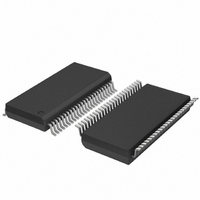
IC UART W/FIFO 48-TSSOP
Manufacturer
NXP Semiconductors
Series
IMPACTr
Datasheet
1.SC28L201A1DGG118.pdf
(110 pages)
Specifications of SC28L201A1DGG,118
Features
False-start Bit Detection
Number Of Channels
2, DUART
Fifo's
256 Byte
Voltage - Supply
3.3V, 5V
With Parallel Port
Yes
With Auto Flow Control
Yes
With False Start Bit Detection
Yes
With Modem Control
Yes
With Cmos
Yes
Mounting Type
Surface Mount
Package / Case
48-TSSOP
Lead Free Status / RoHS Status
Lead free / RoHS Compliant
Other names
935277824118
SC28L201A1DGG-T
SC28L201A1DGG-T
SC28L201A1DGG-T
SC28L201A1DGG-T


Philips Semiconductors
Table 3:
See
6. Functional description
9397 750 13138
Product data sheet
Symbol
I/O6B
I/O4B to I/O2B
I/O0B
V
V
DD
SS
Figure
4.
Pin description for 68000 bus interface (Motorola)
6.1.1 Bus interface: the two basic modes of bus interface
Pin
29
30, 31, 32
33
1, 13, 24,
34
2, 14, 25,
35, 36
6.1 Brief description of functional blocks
Refer to the block diagrams shown in
The SC28L201 is composed of several functional blocks. They are listed in the
approximate order of hierarchy as seen from the pins of the device.
The bus interface operates in ‘68000’ or ‘86xxx’ format as selected by the MODE_IM pin.
The signals used by this section are the Address, Data bus, Chip select, read/write, Data
acknowledge and Interrupt acknowledge and Interrupt request. Assertion of DACKN
requires two edges of the SCLK after the assertion of CEN. The default mode is the
86xxx mode. Pin or register programming may change it to the 68000 mode.
•
•
•
•
•
•
•
•
•
•
•
Bus interface. Motorola or Intel format
Timing circuits
I/O ports
UART
Transmitter and receiver
Transmitter real time error test
FIFO structures
Arbitrating interrupt structure
Character and address recognition
Flow control
Test and software compatibility with previous Philips UARTs
Type
I/O
power
power
Description
Additional general-purpose I/O pins. They are similar to the above without any
connection to the data path or clocks. They have Change-Of-State (COS) detectors
and will generate interrupts if enabled.
Power supply (4 pins). +3.3 V
assured from 2.97 V or 5.5 V. Timing parameters are specified with respect to the
V
Ground (5 pins)
DD
being at 3.3 V
Rev. 01 — 31 October 2005
10 % or 5.0 V
…continued
Figure 1
3.3 V, 5 V UART, 3.125 Mbit/s, with 256-byte FIFO
10 % or +5.0 V
10 %.
and
Figure
2.
© Koninklijke Philips Electronics N.V. 2005. All rights reserved.
10 % supply input. Operation is
SC28L201
9 of 110
Related parts for SC28L201A1DGG,118
Image
Part Number
Description
Manufacturer
Datasheet
Request
R

Part Number:
Description:
NXP Semiconductors designed the LPC2420/2460 microcontroller around a 16-bit/32-bitARM7TDMI-S CPU core with real-time debug interfaces that include both JTAG andembedded trace
Manufacturer:
NXP Semiconductors
Datasheet:

Part Number:
Description:
NXP Semiconductors designed the LPC2458 microcontroller around a 16-bit/32-bitARM7TDMI-S CPU core with real-time debug interfaces that include both JTAG andembedded trace
Manufacturer:
NXP Semiconductors
Datasheet:
Part Number:
Description:
NXP Semiconductors designed the LPC2468 microcontroller around a 16-bit/32-bitARM7TDMI-S CPU core with real-time debug interfaces that include both JTAG andembedded trace
Manufacturer:
NXP Semiconductors
Datasheet:
Part Number:
Description:
NXP Semiconductors designed the LPC2470 microcontroller, powered by theARM7TDMI-S core, to be a highly integrated microcontroller for a wide range ofapplications that require advanced communications and high quality graphic displays
Manufacturer:
NXP Semiconductors
Datasheet:
Part Number:
Description:
NXP Semiconductors designed the LPC2478 microcontroller, powered by theARM7TDMI-S core, to be a highly integrated microcontroller for a wide range ofapplications that require advanced communications and high quality graphic displays
Manufacturer:
NXP Semiconductors
Datasheet:
Part Number:
Description:
The Philips Semiconductors XA (eXtended Architecture) family of 16-bit single-chip microcontrollers is powerful enough to easily handle the requirements of high performance embedded applications, yet inexpensive enough to compete in the market for hi
Manufacturer:
NXP Semiconductors
Datasheet:
Part Number:
Description:
The XA-S3 device is a member of Philips Semiconductors? XA(eXtended Architecture) family of high performance 16-bitsingle-chip microcontrollers
Manufacturer:
NXP Semiconductors
Datasheet:

Part Number:
Description:
The NXP BlueStreak LH75401/LH75411 family consists of two low-cost 16/32-bit System-on-Chip (SoC) devices
Manufacturer:
NXP Semiconductors
Datasheet:
Part Number:
Description:
The NXP LPC3130/3131 combine an 180 MHz ARM926EJ-S CPU core, high-speed USB2
Manufacturer:
NXP Semiconductors
Datasheet:
Part Number:
Description:
The NXP LPC3141 combine a 270 MHz ARM926EJ-S CPU core, High-speed USB 2
Manufacturer:
NXP Semiconductors
Part Number:
Description:
The NXP LPC3143 combine a 270 MHz ARM926EJ-S CPU core, High-speed USB 2
Manufacturer:
NXP Semiconductors

Part Number:
Description:
The NXP LPC3152 combines an 180 MHz ARM926EJ-S CPU core, High-speed USB 2
Manufacturer:
NXP Semiconductors
Part Number:
Description:
The NXP LPC3154 combines an 180 MHz ARM926EJ-S CPU core, High-speed USB 2
Manufacturer:
NXP Semiconductors

Part Number:
Description:
Standard level N-channel enhancement mode Field-Effect Transistor (FET) in a plastic package using NXP High-Performance Automotive (HPA) TrenchMOS technology
Manufacturer:
NXP Semiconductors
Datasheet: