SC28L201A1DGG,118 NXP Semiconductors, SC28L201A1DGG,118 Datasheet - Page 79
SC28L201A1DGG,118
Manufacturer Part Number
SC28L201A1DGG,118
Description
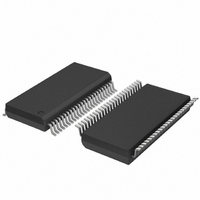
IC UART W/FIFO 48-TSSOP
Manufacturer
NXP Semiconductors
Series
IMPACTr
Datasheet
1.SC28L201A1DGG118.pdf
(110 pages)
Specifications of SC28L201A1DGG,118
Features
False-start Bit Detection
Number Of Channels
2, DUART
Fifo's
256 Byte
Voltage - Supply
3.3V, 5V
With Parallel Port
Yes
With Auto Flow Control
Yes
With False Start Bit Detection
Yes
With Modem Control
Yes
With Cmos
Yes
Mounting Type
Surface Mount
Package / Case
48-TSSOP
Lead Free Status / RoHS Status
Lead free / RoHS Compliant
Other names
935277824118
SC28L201A1DGG-T
SC28L201A1DGG-T
SC28L201A1DGG-T
SC28L201A1DGG-T


Philips Semiconductors
9397 750 13138
Product data sheet
8.6.8 Input Change Detect Enable, B (IPCE)
8.6.9 I/O Port Configuration Registers (I/OPCR0, I/OPCR1, I/OPCR2, I/OPCR3)
IPCE[7:0] bits activate the input change of state detectors. If a pin is configured as an
output, the change of state detectors, if enabled, continue to be active and will show a
change of state as the I/P port changes.
Table 68:
These four registers contain 4 2-bit fields that set the direction and source for each of the
I/O pins associated with the channel. The I/O0B output may be RTSN if MR1[7] is set. It
may also signal end of transmission if MR2[5] is set. (Please see the descriptions of these
functions under
2
The binary settings of the binary 00 combination always configures the I/O pins as
‘inputs’. However, the input circuit of the I/O pins are always active. In actuality, the binary
00 condition only disables the output driver of the pin. Since the input circuit and the
associated change-of-state detector is always active, the output signal may generate
interrupts or drive counters.
This register resets to 0x00 on reset, effectively configuring all I/O pins as inputs. Inputs
may be used as RxC, TxC inputs or CTSN and General Purpose Inputs simultaneously.
All inputs are equipped with change detectors that may be used to generate interrupts or
can be polled, as required.
Remark: Both I/O Port A and B default to input upon a hardware reset to avoid hardware
conflicts with I/O direction.
Bit
7
6
5
4
3
2
1
0
(MR2)”).
Symbol
IPCE - Input Change Detect Enable register, A (address 0x32) bit description
Section 8.2.2 “Mode Register 1 (MR1)”
Description
reserved
reserved
reserved
Rev. 01 — 31 October 2005
I/O6B enable.
I/O4B enable.
I/O3B enable.
I/O2B enable.
I/O0B enable.
0 = disable
1 = enable
0 = disable
1 = enable
0 = disable
1 = enable
0 = disable
1 = enable
0 = disable
1 = enable
3.3 V, 5 V UART, 3.125 Mbit/s, with 256-byte FIFO
and
© Koninklijke Philips Electronics N.V. 2005. All rights reserved.
Section 8.2.3 “Mode Register
SC28L201
79 of 110
Related parts for SC28L201A1DGG,118
Image
Part Number
Description
Manufacturer
Datasheet
Request
R

Part Number:
Description:
NXP Semiconductors designed the LPC2420/2460 microcontroller around a 16-bit/32-bitARM7TDMI-S CPU core with real-time debug interfaces that include both JTAG andembedded trace
Manufacturer:
NXP Semiconductors
Datasheet:

Part Number:
Description:
NXP Semiconductors designed the LPC2458 microcontroller around a 16-bit/32-bitARM7TDMI-S CPU core with real-time debug interfaces that include both JTAG andembedded trace
Manufacturer:
NXP Semiconductors
Datasheet:
Part Number:
Description:
NXP Semiconductors designed the LPC2468 microcontroller around a 16-bit/32-bitARM7TDMI-S CPU core with real-time debug interfaces that include both JTAG andembedded trace
Manufacturer:
NXP Semiconductors
Datasheet:
Part Number:
Description:
NXP Semiconductors designed the LPC2470 microcontroller, powered by theARM7TDMI-S core, to be a highly integrated microcontroller for a wide range ofapplications that require advanced communications and high quality graphic displays
Manufacturer:
NXP Semiconductors
Datasheet:
Part Number:
Description:
NXP Semiconductors designed the LPC2478 microcontroller, powered by theARM7TDMI-S core, to be a highly integrated microcontroller for a wide range ofapplications that require advanced communications and high quality graphic displays
Manufacturer:
NXP Semiconductors
Datasheet:
Part Number:
Description:
The Philips Semiconductors XA (eXtended Architecture) family of 16-bit single-chip microcontrollers is powerful enough to easily handle the requirements of high performance embedded applications, yet inexpensive enough to compete in the market for hi
Manufacturer:
NXP Semiconductors
Datasheet:
Part Number:
Description:
The XA-S3 device is a member of Philips Semiconductors? XA(eXtended Architecture) family of high performance 16-bitsingle-chip microcontrollers
Manufacturer:
NXP Semiconductors
Datasheet:

Part Number:
Description:
The NXP BlueStreak LH75401/LH75411 family consists of two low-cost 16/32-bit System-on-Chip (SoC) devices
Manufacturer:
NXP Semiconductors
Datasheet:
Part Number:
Description:
The NXP LPC3130/3131 combine an 180 MHz ARM926EJ-S CPU core, high-speed USB2
Manufacturer:
NXP Semiconductors
Datasheet:
Part Number:
Description:
The NXP LPC3141 combine a 270 MHz ARM926EJ-S CPU core, High-speed USB 2
Manufacturer:
NXP Semiconductors
Part Number:
Description:
The NXP LPC3143 combine a 270 MHz ARM926EJ-S CPU core, High-speed USB 2
Manufacturer:
NXP Semiconductors

Part Number:
Description:
The NXP LPC3152 combines an 180 MHz ARM926EJ-S CPU core, High-speed USB 2
Manufacturer:
NXP Semiconductors
Part Number:
Description:
The NXP LPC3154 combines an 180 MHz ARM926EJ-S CPU core, High-speed USB 2
Manufacturer:
NXP Semiconductors

Part Number:
Description:
Standard level N-channel enhancement mode Field-Effect Transistor (FET) in a plastic package using NXP High-Performance Automotive (HPA) TrenchMOS technology
Manufacturer:
NXP Semiconductors
Datasheet: