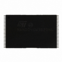
NAND04GW3B2DN6E NUMONYX, NAND04GW3B2DN6E Datasheet - Page 46

NAND04GW3B2DN6E
Manufacturer Part Number
NAND04GW3B2DN6E
Description
IC FLASH 4GBIT 48TSOP
Manufacturer
NUMONYX
Datasheet
1.NAND04GW3B2DN6E.pdf
(72 pages)
Specifications of NAND04GW3B2DN6E
Format - Memory
FLASH
Memory Type
FLASH - Nand
Memory Size
4G (512M x 8)
Interface
Parallel
Voltage - Supply
2.7 V ~ 3.6 V
Operating Temperature
-40°C ~ 85°C
Package / Case
48-TSOP
Lead Free Status / RoHS Status
Lead free / RoHS Compliant
Speed
-
Lead Free Status / RoHS Status
Lead free / RoHS Compliant
Available stocks
Company
Part Number
Manufacturer
Quantity
Price
Company:
Part Number:
NAND04GW3B2DN6E
Manufacturer:
StarMicro
Quantity:
872
Company:
Part Number:
NAND04GW3B2DN6E
Manufacturer:
ST
Quantity:
5 645
Part Number:
NAND04GW3B2DN6E
Manufacturer:
ST
Quantity:
20 000
Software algorithms
9
9.1
46/72
Software algorithms
This section provides information on the software algorithms that Numonyx recommends
implementing to manage the bad blocks and extend the lifetime of the NAND device.
NAND flash memories are programmed and erased by Fowler-Nordheim tunnelling using
high voltage. Exposing the device to high voltage for extended periods damages the oxide
layer.
To extend the number of program and erase cycles and increase the data retention, the:
To help integrate a NAND memory into an application, Numonyx provides a file system OS
native reference software, which supports the basic commands of file management.
Contact the nearest Numonyx sales office for more details.
Bad block management
Devices with bad blocks have the same quality level and the same AC and DC
characteristics as devices that have all valid blocks. A bad block does not affect the
performance of valid blocks because it is isolated from the bit and common source lines by a
select transistor.
The devices are supplied with all the locations inside valid blocks erased (FFh). The bad
block information is written prior to shipping. Any block, where the 1st and 6th bytes (x8
devices) /1st word (x16 devices), in the spare area of the 1st page, does not contain FFh is
a bad block.
The bad block information must be read before any erase is attempted as the bad block
information may be erased. For the system to be able to recognize the bad blocks based on
the original information, the creation of a bad block table following the flowchart shown in
Figure 21: Bad block management flowchart
Number of program and erase cycles is limited
program erase endurance cycles
Implementation of a garbage collection, a wear-leveling algorithm and an error
correction code is recommended.
for the values)
is recommended.
(seeTable 24: Program erase times and
NAND04G-B2D, NAND08G-BxC


