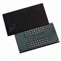
MT48H4M16LFB4-75:H TR Micron Technology Inc, MT48H4M16LFB4-75:H TR Datasheet - Page 26

MT48H4M16LFB4-75:H TR
Manufacturer Part Number
MT48H4M16LFB4-75:H TR
Description
IC SDRAM 64MBIT 133MHZ 54VFBGA
Manufacturer
Micron Technology Inc
Datasheet
1.MT48H4M16LFB4-75_ITH_TR.pdf
(62 pages)
Specifications of MT48H4M16LFB4-75:H TR
Format - Memory
RAM
Memory Type
Mobile SDRAM
Memory Size
64M (4M x 16)
Speed
133MHz
Interface
Parallel
Voltage - Supply
1.7 V ~ 1.9 V
Operating Temperature
0°C ~ 70°C
Package / Case
54-VFBGA
Lead Free Status / RoHS Status
Lead free / RoHS Compliant
Other names
557-1392-2
Figure 19:
Figure 20:
PDF: 09005aef8237ed98/Source: 09005aef8237ed68
64mb_x16_Mobile SDRAM_Y24L_2.fm - Rev. C 10/07 EN
Random WRITE Cycles
WRITE-to-READ
Note:
Note:
either the last of a burst of two or the last desired of a longer burst. Following the
PRECHARGE command, a subsequent command to the same bank cannot be issued
until
In the case of a fixed-length burst being executed to completion, a PRECHARGE
command issued at the optimum time (as described above) provides the same operation
that would result from the same fixed-length burst with auto precharge. The disadvan-
tage of the PRECHARGE command is that it requires that the command and address
buses be available at the appropriate time to issue the command; the advantage of the
PRECHARGE command is that it can be used to truncate fixed-length bursts.
Fixed-length WRITE bursts can be truncated with the BURST TERMINATE command.
When truncating a WRITE burst, the input data applied coincident with the BURST
TERMINATE command will be ignored. The last data written (provided that DQM is
LOW at that time) will be the input data applied one clock previous to the BURST
TERMINATE command. This is shown in Figure 22 on page 27, where data n is the last
desired data element of a longer burst.
Command
Command
Address
Address
Each WRITE command may be issued to any bank. DQM is LOW.
The WRITE command may be issued to any bank, and the READ command may be issued
to any bank. DQM is LOW. CL = 2 for illustration.
CLK
t
DQ
RP is met.
CLK
DQ
Transitioning Data
WRITE
Bank,
Col n
D
T0
WRITE
n
Bank,
Col n
IN
D
T0
n
IN
WRITE
Bank,
Col a
T1
D
a
IN
n + 1
NOP
T1
D
IN
WRITE
Bank,
Col x
D
T2
x
IN
26
Transitioning Data
Bank,
Col b
READ
T2
Don’t Care
WRITE
Bank,
Col m
T3
D
m
IN
Micron Technology, Inc., reserves the right to change products or specifications without notice.
T3
NOP
64Mb: 4 Meg x 16 Mobile SDRAM
NOP
D
T4
OUT
b
Don’t Care
NOP
b + 1
T5
D
OUT
©2006 Micron Technology, Inc. All rights reserved.
Operations


