MCP3909EV-MCU16 Microchip Technology, MCP3909EV-MCU16 Datasheet - Page 33
MCP3909EV-MCU16
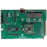
Manufacturer Part Number
MCP3909EV-MCU16
Description
EVALUATION BOARD FOR MCP3909
Manufacturer
Microchip Technology
Datasheets
1.MCP3909T-ISS.pdf
(44 pages)
2.MCP3909T-ISS.pdf
(104 pages)
3.MCP3909EV-MCU16.pdf
(38 pages)
Specifications of MCP3909EV-MCU16
Number Of Adc's
2
Number Of Bits
16
Sampling Rate (per Second)
15k
Data Interface
Serial
Inputs Per Adc
1 Differential
Input Range
±1 V
Voltage Supply Source
Analog and Digital
Operating Temperature
-40°C ~ 85°C
Utilized Ic / Part
MCP3909
Silicon Manufacturer
Microchip
Application Sub Type
ADC
Kit Application Type
Data Converter
Silicon Core Number
MCP3909
Kit Contents
Board
Lead Free Status / RoHS Status
Lead free / RoHS Compliant


3.4
FIGURE 3-3:
3.4.1
© 2009 Microchip Technology Inc.
ADC SAMPLING SCHEME FOR CALCULATIONS
Processing IC1 Interrupt
Sampling
Cycle n
Idle
The ADC conversion rate of the MCP3909 device is determined by the frequency of
master clock, MCLK, and the rate will be MCLK/256. After each conversion is complete,
a DataReady signal (4-CLK length) is generated by the SDO of the MCP3909 device.
The signal is fed into IC1 (Input Capture 1 on the dsPIC33F), allowing the Interrupt
Service Routine (ISR) of IC1 to invoke data-read function of the MCP3909 device.
When the MCP3909 device outputs data, it first sends the ADC result of the voltage
channel, then that of the current channel, with the MSB first.
The frequency of the master clock, MCLK, of the MCP3909 device is 3.2768 MHz, and
ADC outputs @12.8 ksps. In practice 6.4 ksps sampling rate is used in the program,
which means only 1 output data is used for every 2 data sampled. For a 50 Hz input
signal, a 6.4 ksps sampling rate will take 128 samples for each cycle. The active power
calculation is computed based on this condition.
The other parameters for which precision is not critical, such as reactive energy,
voltage, current and frequency, the sampling rate may be reduced to save data storage
space and processing time. In this design, the 3.2 ksps sampling rate is used, which
means only 1 result is stored for every 4 ADC conversions.
In the program, sampling and calculation are carried out concurrently, and data is
stored in the cyclic array in the dsPIC33F RAM. A calculation may be performed after
either 1 cycle, 2 cycles or 3 cycles of data are sampled, which can be configured in the
program. The user should note that frequent calculations will increase the measure-
ment precision at the price of system overhead and response speed, therefore making
proper tradeoffs based on practical requirement. In this design, 3 cycles of signals are
sampled before an AC electrical parameter calculation is performed. Refer to
Figure 3-3.
AC Signal Sampling alnd Computing.
Input capture IC1 is used to detect if the A/D conversion is complete. After each
conversion, a positive pulse the width of 4 clock cycles is outputted by the SDO pin of
the MCP3909 device. IC1 is used to detect the falling edge of the pulse and generate
an interrupt for every 2 falling edges, i.e., 1 data is read for every 2 conversions, thus
realizing 6.4 ksps sampling rate.
In addition to reading the data of the MCP3909 device, the IC1 interrupt service routine
(ISR) also controls the energy pulse output generation. Energy pulse processing
consists of active/reactive energy pulse processing. For the pulses to be outputted
more uniformly, the clock resolution used to generate the pulses must be as high as
possible. The interval of the IC1 interrupt is 156.25 µs, therefore, the resolution
generated by the pulse can be up to 156.25 µs.
Cycle n+1
Sampling
Idle
Cycle n+2
Sampling
Idle
n,n+1,n+2
Calculate
Cycle n+3
Sampling
Cycle n+4
Sampling
Idle
Firmware
DS51723A-page 33
Related parts for MCP3909EV-MCU16
Image
Part Number
Description
Manufacturer
Datasheet
Request
R

Part Number:
Description:
Manufacturer:
Microchip Technology Inc.
Datasheet:
Part Number:
Description:
Manufacturer:
Microchip Technology Inc.
Datasheet:
Part Number:
Description:
Manufacturer:
Microchip Technology Inc.
Datasheet:
Part Number:
Description:
Manufacturer:
Microchip Technology Inc.
Datasheet:
Part Number:
Description:
Manufacturer:
Microchip Technology Inc.
Datasheet:
Part Number:
Description:
Manufacturer:
Microchip Technology Inc.
Datasheet:
Part Number:
Description:
Manufacturer:
Microchip Technology Inc.
Datasheet:
Part Number:
Description:
Manufacturer:
Microchip Technology Inc.
Datasheet: