MCP3909EV-MCU16 Microchip Technology, MCP3909EV-MCU16 Datasheet - Page 98
MCP3909EV-MCU16
Manufacturer Part Number
MCP3909EV-MCU16
Description
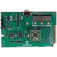
EVALUATION BOARD FOR MCP3909
Manufacturer
Microchip Technology
Datasheets
1.MCP3909T-ISS.pdf
(44 pages)
2.MCP3909T-ISS.pdf
(104 pages)
3.MCP3909EV-MCU16.pdf
(38 pages)
Specifications of MCP3909EV-MCU16
Number Of Adc's
2
Number Of Bits
16
Sampling Rate (per Second)
15k
Data Interface
Serial
Inputs Per Adc
1 Differential
Input Range
±1 V
Voltage Supply Source
Analog and Digital
Operating Temperature
-40°C ~ 85°C
Utilized Ic / Part
MCP3909
Silicon Manufacturer
Microchip
Application Sub Type
ADC
Kit Application Type
Data Converter
Silicon Core Number
MCP3909
Kit Contents
Board
Lead Free Status / RoHS Status
Lead free / RoHS Compliant


MCP3909 / dsPIC33F 3-Phase Energy Meter Reference Design
C.16 PHASE LAG COMPENSATION
DS51723A-page 98
Phase lag of a CT has no effect on the metering of RMS current/voltage and apparent
power, but will affect the metering of power, since the phase lag will change the phase
relationship between the input current and the voltage. This will result in a deviation of
the calculated active power from the calculated reactive power.
Figure C-10 shows how a transformer's phase lag affects the measured results under
both inductive and capacitive loads. Let's assume that the output of CT has no phase
lag from the input voltage, while the CT has a phase lag from the input signal. With
inductive loads, the phase angle increases between the volatge and the current
because of the phase lag induced by the CT, resulting in a decrease of the measured
active power and an increase of the reactive power. While with capacitive loads, the
phase angle between the voltage and the current decreases because of the phase lag
induced by the CT, resulting in a decrease of the measured reactive power and an
increase of active power.
There are many methods for phase lag compensation. In this design the result correc-
tion method is used. It compensates with a coefficient after the active power and
reactive power are figured out, which has a small amount of calculation.
FIGURE C-10:
Assuming that the phase lag of CT is ϕ
phase lag between current and voltage is:
FIGURE C-11:
Inductive
Capacitive
Load
Load
θ
Δθ
Measurement Change Caused By Transformer Phase Lag.
Principle Of Phase Lag Correction.
Δf
CT Output
current
current
voltage
Input
Input
F
S
P'
P
i
, of PT is ϕ
Δϕ
=
ϕ
u
–
u
, after PT and CT, the variation of
ϕ
Inductive
Capacitive
i
.
Load
Load
Q
© 2009 Microchip Technology Inc.
θ
Q'
Δθ
current
Input
voltage
Input
CT Output
current
Related parts for MCP3909EV-MCU16
Image
Part Number
Description
Manufacturer
Datasheet
Request
R

Part Number:
Description:
Manufacturer:
Microchip Technology Inc.
Datasheet:
Part Number:
Description:
Manufacturer:
Microchip Technology Inc.
Datasheet:
Part Number:
Description:
Manufacturer:
Microchip Technology Inc.
Datasheet:
Part Number:
Description:
Manufacturer:
Microchip Technology Inc.
Datasheet:
Part Number:
Description:
Manufacturer:
Microchip Technology Inc.
Datasheet:
Part Number:
Description:
Manufacturer:
Microchip Technology Inc.
Datasheet:
Part Number:
Description:
Manufacturer:
Microchip Technology Inc.
Datasheet:
Part Number:
Description:
Manufacturer:
Microchip Technology Inc.
Datasheet: