EVAL-ADT7467EB Analog Devices Inc, EVAL-ADT7467EB Datasheet - Page 34
EVAL-ADT7467EB
Manufacturer Part Number
EVAL-ADT7467EB
Description
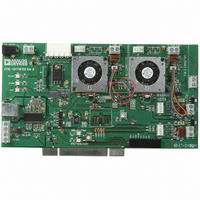
BOARD EVALUATION FOR ADT7467
Manufacturer
Analog Devices Inc
Series
dBCool®r
Datasheet
1.EVAL-ADT7467EB.pdf
(80 pages)
Specifications of EVAL-ADT7467EB
Sensor Type
Temperature
Sensing Range
-40°C ~ 120°C
Interface
SMBus (2-Wire/I²C)
Sensitivity
±1.5°C
Voltage - Supply
3 V ~ 5.5 V
Embedded
No
Utilized Ic / Part
ADT7467
Lead Free Status / RoHS Status
Contains lead / RoHS non-compliant


ADT7467
MISCELLANEOUS FUNCTIONS
OPERATING FROM 3.3 V STANDBY
The ADT7467 has been specifically designed to operate from a
3.3 V STBY supply. In computers that support S3 and S5 states,
the core voltage of the processor is lowered in these states. If
using the dynamic T
processor changes the CPU temperature and changes the
dynamics of the system under dynamic T
when monitoring THERM , the THERM timer should be
disabled during these states.
Dynamic T
When the power is supplied from 3.3 V STBY and the V
voltage drops below the V
1.
2.
3.
4.
5.
Once the core voltage, V
everything is re-enabled and the system resumes normal
operation.
XNOR TREE TEST MODE
The ADT7467 includes an XNOR tree test mode. This mode is
useful for in-circuit test equipment at board-level testing. By
applying stimulus to the pins included in the XNOR tree, it is
possible to detect opens or shorts on the system board.
Figure 47 shows the signals that are exercised in the XNOR tree
test mode. The XNOR tree test is invoked by setting Bit 0
(XEN) of the XNOR tree test enable register (Reg. 0x6F).
Status Bit 1 (V
SMBALERT is generated if enabled.
THERM monitoring is disabled. The THERM timer
should hold its value prior to the S3 or S5 state.
Dynamic T
being adjusted due to an S3 or S5 state.
The ADT7467 is prevented from shutting down.
MIN
Control Register 1 (Reg. 0x36) <1> V
MIN
TACH1
TACH2
TACH3
TACH4
CCP
PWM2
PWM3
control is disabled. This prevents T
MIN
Figure 47. XNOR Tree Test
) in Status Register 1 is set.
mode, lowering the core voltage of the
CCP
CCP
, goes above the V
low limit, the following occurs:
PWM1/XTO
MIN
control. Likewise,
CCP
low limit,
CCP
MIN
CCP
LO = 1
from
Rev. A | Page 34 of 80
POWER-ON DEFAULT
When the ADT7467 is powered up, it polls the V
If V
powered up), the ADT7467 assumes the functionality of the
default registers after the ADT7467 is addressed via any valid
SMBus transaction.
If V
up), a fail-safe timer begins to count down. If the ADT7467 is
not addressed by a valid SMBus transaction before the fail-safe
timeout (4.6 sec) lapses, the ADT7467 drives the fans to full
speed. If the ADT7467 is addressed by a valid SMBus
transaction after this point, the fans stop and the ADT7467
assumes its default settings and begins normal operation.
If V
up), a fail-safe timer begins to count down. If the ADT7467 is
addressed by a valid SMBus transaction before the fail-safe
timeout (4.6 sec) lapses, the ADT7467 operates normally,
assuming the functionality of all default registers. See the flow
chart in Figure 48.
Y
Y
AFTER THE FAIL-SAFE TIMEOUT
CCP
CC
CCP
FAIL-SAFE TIMER ELAPSES
ADT7467 IS POWERED UP
goes high (the system processor power rail is powered
START FAIL-SAFE TIMER
HAS THE ADT7467 BEEN
SMBUS TRANSACTION?
HAS THE ADT7467 BEEN
SMBUS TRANSACTION?
HAS THE ADT7467 BEEN
SMBUS TRANSACTION?
stays below 0.75 V (the system CPU power rail is not
goes high (the system processor power rail is powered
ACCESSED BY A VALID
ACCESSED BY A VALID
ACCESSED BY A VALID
IS V
ADT7467 NORMALLY
CCP
START UP THE
ABOVE 0.75V?
N
Y
N
Y
Figure 48. Power-On Flowchart
N
N
RUN THE FANS TO FULL SPEED
HAS THE ADT7467 BEEN
SMBUS TRANSACTION?
ACCESSED BY A VALID
SWITCH OFF FANS
CHECK V
Y
CCP
CCP
input.
N
Related parts for EVAL-ADT7467EB
Image
Part Number
Description
Manufacturer
Datasheet
Request
R


Part Number:
Description:
BOARD EVAL FOR SI270X-A
Manufacturer:
Silicon Laboratories Inc
Datasheet:

Part Number:
Description:
BUCK CONV REF DESIGN KIT IP1201
Manufacturer:
International Rectifier
Datasheet:
Part Number:
Description:
BOARD DEMO SYNC DUAL BUCK CNVTER
Manufacturer:
International Rectifier
Datasheet:
Part Number:
Description:
BOARD DEMO SYNC BUCK CONVETER
Manufacturer:
International Rectifier
Datasheet:

Part Number:
Description:
EVALBOARD/EB Omnidirectional microphone - Analog
Manufacturer:
Analog Devices
Datasheet:
Part Number:
Description:
EVALBOARD/EB Omnidirectional microphone - Analog
Manufacturer:
Analog Devices
Datasheet:


Part Number:
Description:
BOARD EVAL LED DRIVER LT3756
Manufacturer:
Linear Technology
Datasheet:

Part Number:
Description:
BOARD EVAL FOR AD7741/7742
Manufacturer:
Analog Devices Inc
Datasheet:

Part Number:
Description:
±1.7g Dual-Axis IMEMS Accelerometer Evaluation Board
Manufacturer:
Analog Devices Inc
Datasheet:

Part Number:
Description:
IC MULTIPLIER ANALOG 8-SOIC T/R
Manufacturer:
Analog Devices Inc
Datasheet:

Part Number:
Description:
IC ANALOG MULTIPLIER 8-DIP
Manufacturer:
Analog Devices Inc
Datasheet:
Part Number:
Description:
IC ANALOG MULTIPLIER 8-SOIC
Manufacturer:
Analog Devices Inc
Datasheet:
Part Number:
Description:
IC ANALOG MULTIPLIER 8-DIP
Manufacturer:
Analog Devices Inc
Datasheet: