EVAL-ADT7467EB Analog Devices Inc, EVAL-ADT7467EB Datasheet - Page 65
EVAL-ADT7467EB
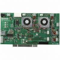
Manufacturer Part Number
EVAL-ADT7467EB
Description
BOARD EVALUATION FOR ADT7467
Manufacturer
Analog Devices Inc
Series
dBCool®r
Datasheet
1.EVAL-ADT7467EB.pdf
(80 pages)
Specifications of EVAL-ADT7467EB
Sensor Type
Temperature
Sensing Range
-40°C ~ 120°C
Interface
SMBus (2-Wire/I²C)
Sensitivity
±1.5°C
Voltage - Supply
3 V ~ 5.5 V
Embedded
No
Utilized Ic / Part
ADT7467
Lead Free Status / RoHS Status
Contains lead / RoHS non-compliant


Table 26. Register 0x40—Configuration Register 1 (Power-On Default = 0x01)
Bit
<0>
<1>
<2>
<3>
<4>
<5>
<6>
<7>
Table 27. Register 0x41—Interrupt Status Register 1 (Power-On Default = 0x00)
Bit
<1>
<2>
<4>
<5>
<6>
<7>
Name
STRT
LOCK
RDY
FSPD
VxI
FSPDIS
TODIS
V
Name
V
V
R1T
LT
R2T
OOL
CC
CCP
CC
R/W
Read only
Read only
Read only
Read only
Read only
Read only
R/W
Read/write
Write once
Read only
Read/write
Read/write
Read/write
Read/write
Read/write
Description
V
status register if the error condition has subsided.
V
register if the error condition has subsided.
R1T = 1 indicates that the Remote 1 low or high temperature has been exceeded. This bit is cleared upon a
read of the status register if the error condition has subsided.
LT = 1 indicates that the local low or high temperature has been exceeded. This bit is cleared upon a read of
the status register if the error condition has subsided.
R2T = 1 indicates that the Remote 2 low or high temperature has been exceeded. This bit is cleared upon a
read of the status register if the error condition has subsided.
OOL = 1 indicates that an out-of-limit event has been latched in Status Register 2. This bit is a logical OR of all
status bits in Status Register 2. Software can test this bit in isolation to determine whether any of the voltage,
temperature, or fan speed readings represented by Status Register 2 are out-of-limits, which eliminates the
need to read Status Register 2 at every interrupt or in every polling cycle.
Description
Logic 1 enables monitoring and PWM control outputs based on the limit settings programmed.
Logic 0 disables monitoring and PWM control based on the default power-up limit settings.
Note that the limit values programmed are preserved even if a Logic 0 is written to this bit and the default
settings are enabled. This bit becomes a read-only bit and cannot be changed once Bit 1 (LOCK bit) has been
written. All limit registers should be programmed by BIOS before setting this bit to 1. (Lockable)
Logic 1 locks all limit values to their current settings. Once this bit is set, all lockable registers become read-
only registers and cannot be modified until the ADT7467 is powered down and powered up again. This
prevents rogue programs such as viruses from modifying critical system limit settings. (Lockable)
This bit is only set to 1 by the ADT7467 to indicate that the device is fully powered up and ready to begin
system monitoring.
When set to 1, this bit runs all fans at full speed. Power-on default = 0. This bit cannot be locked at any time.
BIOS should set this bit to a 1 when the ADT7467 is configured to measure current from an ADI ADOPT™
VRM controller and to measure the CPU’s core voltage. This bit allows monitoring software to display the
watts used by the CPU. (Lockable)
Logic 1 disables fan spin-up for two TACH pulses, and the PWM outputs go high for the entire fan spin-up
timeout selected.
When this bit is set to 1, the SMBus timeout feature is enabled. This allows the ADT7467 to be used with
SMBus controllers that cannot handle SMBus timeouts. (Lockable)
When this bit is set to 1, the ADT7467 rescales its V
measures V
CCP
CC
= 1 indicates that the V
= 1 indicates that the V
CC
as a 3.3 V supply. (Lockable)
CC
CCP
high or low limit has been exceeded. This bit is cleared upon a read of the status
high or low limit has been exceeded. This bit is cleared upon a read of the
Rev. A | Page 65 of 80
CC
pin to measure 5 V supply. If this bit is 0, the ADT7467
ADT7467
Related parts for EVAL-ADT7467EB
Image
Part Number
Description
Manufacturer
Datasheet
Request
R


Part Number:
Description:
BOARD EVAL FOR SI270X-A
Manufacturer:
Silicon Laboratories Inc
Datasheet:

Part Number:
Description:
BUCK CONV REF DESIGN KIT IP1201
Manufacturer:
International Rectifier
Datasheet:
Part Number:
Description:
BOARD DEMO SYNC DUAL BUCK CNVTER
Manufacturer:
International Rectifier
Datasheet:
Part Number:
Description:
BOARD DEMO SYNC BUCK CONVETER
Manufacturer:
International Rectifier
Datasheet:

Part Number:
Description:
EVALBOARD/EB Omnidirectional microphone - Analog
Manufacturer:
Analog Devices
Datasheet:
Part Number:
Description:
EVALBOARD/EB Omnidirectional microphone - Analog
Manufacturer:
Analog Devices
Datasheet:


Part Number:
Description:
BOARD EVAL LED DRIVER LT3756
Manufacturer:
Linear Technology
Datasheet:

Part Number:
Description:
BOARD EVAL FOR AD7741/7742
Manufacturer:
Analog Devices Inc
Datasheet:

Part Number:
Description:
±1.7g Dual-Axis IMEMS Accelerometer Evaluation Board
Manufacturer:
Analog Devices Inc
Datasheet:

Part Number:
Description:
IC MULTIPLIER ANALOG 8-SOIC T/R
Manufacturer:
Analog Devices Inc
Datasheet:

Part Number:
Description:
IC ANALOG MULTIPLIER 8-DIP
Manufacturer:
Analog Devices Inc
Datasheet:
Part Number:
Description:
IC ANALOG MULTIPLIER 8-SOIC
Manufacturer:
Analog Devices Inc
Datasheet:
Part Number:
Description:
IC ANALOG MULTIPLIER 8-DIP
Manufacturer:
Analog Devices Inc
Datasheet: