ADZS-BF527-EZLITE Analog Devices Inc, ADZS-BF527-EZLITE Datasheet
ADZS-BF527-EZLITE
Specifications of ADZS-BF527-EZLITE


Related parts for ADZS-BF527-EZLITE


ADZS-BF527-EZLITE Summary of contents
Page 1
Preliminary Technical Data FEATURES Up to 600 MHz high-performance Blackfin processor Two 16-bit MACs, two 40-bit ALUs, four 8-bit video ALUs, 40-bit shifter RISC-like register and instruction model for ease of programming and compiler-friendly support Advanced debug, trace, and performance ...
Page 2
ADSP-BF522/523/524/525/526/527 TABLE OF CONTENTS General Description ................................................. 3 Portable Low-Power Architecture ............................. 3 System Integration ................................................ 3 Processor Peripherals ............................................. 3 Blackfin Processor Core .......................................... 4 Memory Architecture ............................................ 5 DMA Controllers .................................................. 9 Host DMA Port .................................................... 9 Real-Time ...
Page 3
Preliminary Technical Data GENERAL DESCRIPTION The ADSP-BF522/524/526 and ADSP-BF523/525/527 proces- sors are members of the Blackfin family of products, incorporating the Analog Devices/Intel Micro Signal Architec- ture (MSA). Blackfin processors combine a dual-MAC state-of- the-art signal processing engine, the advantages ...
Page 4
ADSP-BF522/523/524/525/526/527 The ADSP-BF523/525/527 processors include an on-chip volt- age regulator in support of the processor’s dynamic power management capability. The voltage regulator provides a range of core voltage levels when supplied from V regulator can be bypassed at the user's ...
Page 5
Preliminary Technical Data The address arithmetic unit provides two addresses for simulta- neous dual fetches from memory. It contains a multiported register file consisting of four sets of 32-bit index, modify, length, and base registers (for circular buffering), and eight ...
Page 6
ADSP-BF522/523/524/525/526/527 The SDRAM controller can be programmed to interface 128M bytes of SDRAM. A separate row can be open for each SDRAM internal bank and the SDRAM controller supports internal SDRAM banks, improving overall ...
Page 7
Preliminary Technical Data controller to prioritize and control all system events. Conceptu- ally, interrupts from the peripherals enter into the SIC and are then routed directly into the general-purpose interrupts of the CEC. Core Event Controller (CEC) The CEC supports ...
Page 8
ADSP-BF522/523/524/525/526/527 Table 3. System Interrupt Controller (SIC) (Continued) Peripheral Interrupt Event DMA10 Channel (UART1 RX) DMA11 Channel (UART1 TX) OTP Memory Interrupt GP Counter DMA1 Channel (MAC RX/HOSTDP) Port H Interrupt A DMA2 Channel (MAC TX/NFC) Port H Interrupt B ...
Page 9
Preliminary Technical Data The SIC allows further control of event processing by providing three pairs of 32-bit interrupt control and status registers. Each register contains a bit corresponding to each of the peripheral interrupt events shown in Table 3 on ...
Page 10
ADSP-BF522/523/524/525/526/527 REAL-TIME CLOCK The real-time clock (RTC) provides a robust set of digital watch features, including current time, stopwatch, and alarm. The RTC is clocked by a 32.768 kHz crystal external to the Blackfin processor. The RTC peripheral has dedicated ...
Page 11
Preliminary Technical Data SERIAL PORTS The processors incorporate two dual-channel synchronous serial ports (SPORT0 and SPORT1) for serial and multiproces- sor communications. The SPORTs support the following features: 2 • capable operation. • Bidirectional operation – Each SPORT ...
Page 12
ADSP-BF522/523/524/525/526/527 In conjunction with the general-purpose timer functions, auto- baud detection is supported. The capabilities of the UARTs are further extended with sup- port for the infrared data association (IrDA®) serial infrared physical layer link specification (SIR) protocol. TWI CONTROLLER ...
Page 13
Preliminary Technical Data default. Each general-purpose port pin can be individually con- trolled by manipulation of the port control, status, and interrupt registers: • GPIO direction control register – Specifies the direction of each individual GPIO pin as input or ...
Page 14
ADSP-BF522/523/524/525/526/527 Vertical Blanking Interval Mode In this mode, the PPI only transfers vertical blanking interval (VBI) data. Entire Field Mode In this mode, the entire incoming bit stream is read in through the PPI. This includes active video, control preamble ...
Page 15
Preliminary Technical Data Deep Sleep Operating Mode—Maximum Dynamic Power Savings The deep sleep mode maximizes dynamic power savings by dis- abling the clocks to the processor core (CCLK) and to all synchronous peripherals (SCLK). Asynchronous peripherals, such as the RTC, ...
Page 16
ADSP-BF522/523/524/525/526/527 consumption, the internal voltage regulator can be programmed to remove power to the processor core while keeping I/O power supplied. While in the hibernate state, all external supplies ( can still be ...
Page 17
Preliminary Technical Data specified by the crystal manufacturer. The user should verify the customized values based on careful investigations on multiple devices over temperature range. BLACKFIN CLKOUT TO PLL CIRCUITRY EN CLKBUF 560 EN CLKIN XTAL 330 * 18 pF ...
Page 18
ADSP-BF522/523/524/525/526/527 The maximum CCLK frequency not only depends on the part's speed grade (see Page 80), it also depends on the applied V voltage. See Table 12 and Table 15 for details. The maximal sys- tem clock rate (SCLK) depends ...
Page 19
Preliminary Technical Data 2 version 2. multiplexer can be used to select one processor at a time when booting multiple processors from a single TWI. • Boot from UART0 host on Port G (BMODE = 0x7) — ...
Page 20
ADSP-BF522/523/524/525/526/527 For devices consisting of a five-byte signature, only four are read. The fourth must comply as outlined above. Large page devices must support the following command set: —Reset: 0xFF —Read Electronic Signature: 0x90 —Read: 0x00, 0x30 (confirm command) Large-page ...
Page 21
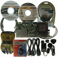
... EZ-KIT Lite® Evaluation Board For evaluation of ADSP-BF522/524/526 and ADSP-BF523/525/527 processors, use the EZ-KIT Lite boards available from Analog Devices. Order using part numbers ADZS-BF526-EZLITE or ADZS-BF527-EZLITE. The boards come with on-chip emulation capabilities and is equipped to enable software development. Multiple daughter cards are available. ...
Page 22
ADSP-BF522/523/524/525/526/527 SIGNAL DESCRIPTIONS Signal definitions for the ADSP-BF522/524/526 and ADSP-BF523/525/527 processors are listed in to maintain maximum function and reduce package size and ball count, some balls have dual, multiplexed functions. In cases where ball function is reconfigurable, the default ...
Page 23
Preliminary Technical Data Table 10. Signal Descriptions (Continued) Signal Name USB 2.0 HS OTG USB_DP USB_DM USB_XI USB_XO USB_ID USB_VREF USB_RSET USB_VBUS Port F: GPIO and Multiplexed Peripherals PF0/PPI D0/DR0PRI /ND_D0A PF1/PPI D1/RFS0/ND_D1A PF2/PPI D2/RSCLK0/ND_D2A PF3/PPI D3/DT0PRI/ND_D3A PF4/PPI D4/TFS0/ND_D4A/TACLK0 PF5/PPI ...
Page 24
ADSP-BF522/523/524/525/526/527 Table 10. Signal Descriptions (Continued) Signal Name PG0/HWAIT PG1/SPISS/SPISEL1 PG2/SCK PG3/MISO/DR0SECA PG4/MOSI/DT0SECA PG5/TMR1/PPI_FS2 PG6/DT0PRIA/TMR2/PPI_FS3 PG7/TMR3/DR0PRIA/UART0TX PG8/TMR4/RFS0A/UART0RX/TACI4 PG9/TMR5/RSCLK0A/TACI5 PG10/TMR6/TSCLK0A/TACI6 PG11/TMR7/HOST_WR PG12/DMAR1/UART1TXA/HOST_ACK PG13/DMAR0/UART1RXA/HOST_ADDR/TACI2 PG14/TSCLK0A1/MDC/HOST_RD 3 PG15 /TFS0A/MII PHYINT/RMII MDINT/HOST_CE I/O Port H: GPIO and Multiplexed Peripherals PH0/ND_D0/MIICRS/RMIICRSDV/HOST_D0 PH1/ND_D1/ERxER/HOST_D1 PH2/ND_D2/MDIO/HOST_D2 PH3/ND_D3/ETxEN/HOST_D3 PH4/ND_D4/MIITxCLK/RMIIREF_CLK/HOST_D4 ...
Page 25
Preliminary Technical Data Table 10. Signal Descriptions (Continued) Signal Name Port J: Multiplexed Peripherals PJ0: PPI_FS1/TMR0 PJ1: PPI_CLK/TMRCLK PJ2: SCL PJ3: SDA Real Time Clock RTXI RTXO JTAG Port TCK TDO TDI TMS TRST EMU Clock CLKIN XTAL CLKBUF Mode ...
Page 26
ADSP-BF522/523/524/525/526/527 Table 10. Signal Descriptions (Continued) Signal Name Power Supplies V DDEXT V DDINT V DDRTC V DDUSB V DDMEM V DDOTP V PPOTP See Output Drive Currents on Page 64 for more information about each driver ...
Page 27
Preliminary Technical Data SPECIFICATIONS Specifications are subject to change without notice. OPERATING CONDITIONS FOR ADSP-BF522/524/526 Parameter V Internal Supply Voltage DDINT 1 V External Supply Voltage DDEXT 2 V RTC Power Supply Voltage DDRTC 3 V MEM Supply Voltage DDMEM ...
Page 28
ADSP-BF522/523/524/525/526/527 Table 11 shows settings for TWI_DT in the NONGPIO_DRIVE register. Set this register prior to using the TWI port. Table 11. TWI_DT Field Selections and V TWI_DT V Nominal DDEXT 1 000 (default) 3.3 001 1.8 010 2.5 011 ...
Page 29
Preliminary Technical Data OPERATING CONDITIONS FOR ADSP-BF523/525/527 Parameter 1 V Internal Supply Voltage DDINT External Supply Voltage DDEXT External Supply Voltage DDEXT V RTC Power Supply Voltage DDRTC MEM Supply Voltage ...
Page 30
ADSP-BF522/523/524/525/526/527 ADSP-BF523/525/527 Clock Related Operating Conditions Table 15 describes the core clock timing requirements for the ADSP-BF523/525/527 processors. Take care in selecting MSEL, SSEL, and CSEL ratios so as not to exceed the maximum core clock and system clock (see ...
Page 31
Preliminary Technical Data ELECTRICAL CHARACTERISTICS Table 18. Common Electrical Characteristics For All ADSP-BF522/523/524/525/526/527 Processors Parameter V High Level Output Voltage OH V High Level Output Voltage OH V High Level Output Voltage OH V Low Level Output Voltage OL I ...
Page 32
ADSP-BF522/523/524/525/526/527 Table 19. Electrical Characteristics For ADSP-BF522/524/526 Processors (Continued) Parameter Hibernate State Current DDHIBERNATE I V Current DDRTC DDRTC I V Current in Full/Low DDUSB-FS DDUSB Speed Mode I V Current in High Speed DDUSB-HS DDUSB Mode ...
Page 33
Preliminary Technical Data Table 20. Electrical Characteristics For ADSP-BF523/525/527 Processors (Continued) Parameter Hibernate State Current DDHIBERNATE I V Current DDRTC DDRTC I V Current in Full/Low DDUSB-FS DDUSB Speed Mode I V Current in High Speed DDUSB-HS ...
Page 34
ADSP-BF522/523/524/525/526/527 Table 22. ADSP-BF522/524/526 Static Current - (°C) TBD V TBD V J –40 TBD TBD –20 TBD TBD 0 TBD TBD 25 TBD TBD 40 TBD TBD 55 TBD TBD 70 TBD TBD 85 TBD TBD ...
Page 35
Preliminary Technical Data Table 24. ADSP-BF522/524/526 Dynamic Current in CCLK Domain (mA, with ASF = 1.0) f CCLK 2 (MHz) TBD V TBD V 400 TBD TBD 300 TBD TBD 200 TBD TBD 100 TBD TBD 1 The values are ...
Page 36
ADSP-BF522/523/524/525/526/527 ABSOLUTE MAXIMUM RATINGS Stresses greater than those listed in the table may cause perma- nent damage to the device. These are stress ratings only. Functional operation of the device at these or any other condi- tions greater than those ...
Page 37
Preliminary Technical Data ESD SENSITIVITY ESD (electrostatic discharge) sensitive device. Charged devices and circuit boards can discharge without detection. Although this product features patented or proprietary circuitry, damage may occur on devices subjected to high energy ESD. Therefore, proper ESD ...
Page 38
ADSP-BF522/523/524/525/526/527 TIMING SPECIFICATIONS Clock and Reset Timing Table 30 and Figure 9 describe clock and reset operations. Per the CCLK and SCLK timing specifications in Table 17, combinations of CLKIN and clock multipliers must not select core/peripheral clocks in excess ...
Page 39
Preliminary Technical Data Asynchronous Memory Read Cycle Timing Table 31. Asynchronous Memory Read Cycle Timing Parameter Timing Requirements t DATA15–0 Setup Before CLKOUT SDAT t DATA15–0 Hold After CLKOUT HDAT t ARDY Setup Before CLKOUT SARDY t ARDY Hold After ...
Page 40
ADSP-BF522/523/524/525/526/527 Asynchronous Memory Write Cycle Timing Table 32. Asynchronous Memory Write Cycle Timing Parameter Timing Requirements t ARDY Setup Before CLKOUT SARDY t ARDY Hold After CLKOUT HARDY Switching Characteristics t DATA15–0 Disable After CLKOUT DDAT t DATA15–0 Enable After ...
Page 41
Preliminary Technical Data NAND Flash Controller Interface Timing Table 33 and Figure 12 on Page 41 through Page 43 describe NAND Flash Controller Interface operations. Table 33. NAND Flash Controller Interface Timing Parameter Write Cycle Switching Characteristics t ND_CE Setup ...
Page 42
ADSP-BF522/523/524/525/526/527 ND_CE ND_CLE ND_ALE AWE ND_D ND_CE ND_CLE ND_ALE AWE ARE ND_D Figure 14. NAND Flash Controller Interface Timing - Data Write Operation t CWL t CLEWL t ALEWL t ALH ...
Page 43
Preliminary Technical Data ND_CE ND_CLE ND_ALE AWE ARE ND_D Figure 15. NAND Flash Controller Interface Timing - Data Read Operation ND_CE ND_CLE ND_ALE AWE ARE ND_D Figure 16. NAND Flash Controller Interface Timing - ...
Page 44
ADSP-BF522/523/524/525/526/527 SDRAM Interface Timing Table 34. SDRAM Interface Timing Parameter Timing Requirements t Data Setup Before CLKOUT SSDAT t Data Hold After CLKOUT HSDAT Switching Characteristics 1 t CLKOUT Period SCLK t CLKOUT Width High SCLKH t CLKOUT Width Low ...
Page 45
Preliminary Technical Data External DMA Request Timing Table 35 and Figure 18 describe the External DMA Request operations. Table 35. External DMA Request Timing Parameter Timing Parameters t DMARx Asserted to CLKOUT High Setup DR t CLKOUT High to DMARx ...
Page 46
ADSP-BF522/523/524/525/526/527 Parallel Peripheral Interface Timing Table 36 and Figure 19 on Page 46, Figure 23 on Page Figure 25 on Page 51 describe parallel peripheral interface operations. Table 36. Parallel Peripheral Interface Timing Parameter Timing Requirements 1 t PPI_CLK Width ...
Page 47
Preliminary Technical Data DATA DRIVING/ FRAME SYNC SAMPLING EDGE PPI_CLK POLC = 0 PPI_CLK POLC = 1 POLS = 1 PPI_FS1 POLS = 0 POLS = 1 PPI_FS2 POLS = 0 PPI_DATA POLC = 0 PPI_CLK PPI_CLK POLC = 1 ...
Page 48
ADSP-BF522/523/524/525/526/527 FRAME SYNC IS DRIVEN OUT PPI_CLK POLC = 0 PPI_CLK POLC = 1 t DFSPE t HOFSPE POLS = 1 PPI_FS1 POLS = 0 POLS = 1 PPI_FS2 POLS = 0 PPI_DATA DATA0 IS DRIVEN OUT t DDTPE t ...
Page 49
Preliminary Technical Data Serial Ports Table 37 through Table 40 on Page 51 and through Figure 25 on Page 51 describe serial port operations. Table 37. Serial Ports—External Clock Parameter Timing Requirements t TFSx/RFSx Setup Before TSCLKx/RSCLKx SFSE t TFSx/RFSx ...
Page 50
ADSP-BF522/523/524/525/526/527 DATA RECEIVE—INTERNAL CLOCK DRIVE EDGE t SCLKIW RSCLKx t DFSI t t HOFSI SFSI RFSx t SDRI DRx NOTE: EITHER THE RISING EDGE OR FALLING EDGE OF RSCLKx OR TSCLKx CAN BE USED AS THE ACTIVE SAMPLING EDGE. DATA ...
Page 51
Preliminary Technical Data Table 40. Serial Ports — External Late Frame Sync Parameter Switching Characteristics t Data Delay from Late External TFSx DDTLFSE or External RFSx in multi-channel mode with MFD = 0 t Data Enable from External RFSx in ...
Page 52
ADSP-BF522/523/524/525/526/527 Serial Peripheral Interface (SPI) Port—Master Timing Table 41 and Figure 26 describe SPI port master operations. Table 41. Serial Peripheral Interface (SPI) Port—Master Timing Parameter Timing Requirements t Data Input Valid to SCK Edge (Data SSPIDM Input Setup) t ...
Page 53
Preliminary Technical Data Serial Peripheral Interface (SPI) Port—Slave Timing Table 42 and Figure 27 describe SPI port slave operations. Table 42. Serial Peripheral Interface (SPI) Port—Slave Timing Parameter Timing Requirements t Serial Clock High Period SPICHS t Serial Clock Low ...
Page 54
ADSP-BF522/523/524/525/526/527 Universal Serial Bus (USB) On-The-Go—Receive and Transmit Timing Table 43 describes the USB On-The-Go receive and transmit operations. Table 43. USB On-The-Go—Receive and Transmit Timing Parameter Timing Requirements f USB_XI Frequency USBS FS USB_XI Clock Frequency Stability USB Universal ...
Page 55
Preliminary Technical Data General-Purpose Port Timing Table 44 and Figure 29 describe general-purpose port operations. Table 44. General-Purpose Port Timing Parameter Timing Requirement t General-Purpose Port Ball Input Pulse Width t WFI Switching Characteristics t General-Purpose Port Ball Output Delay ...
Page 56
ADSP-BF522/523/524/525/526/527 Timer Cycle Timing Table 45 and Figure 30 describe timer expired operations. The input signal is asynchronous in “width capture mode” and “external clock mode” and has an absolute maximum input fre- quency of (f /2) MHz. SCLK Table ...
Page 57
Preliminary Technical Data Timer Clock Timing Table 46 and Figure 31 describe timer clock timing. Table 46. Timer Clock Timing Parameter Switching Characteristic t Timer Output Update Delay After PPI_CLK High TODP PPI_CLK TMRx OUTPUT Up/Down Counter/Rotary Encoder Timing Table ...
Page 58
ADSP-BF522/523/524/525/526/527 HOSTDP A/C Timing- Host Read Cycle Table 48 describe the HOSTDP A/C Host Read Cycle timing requirements. Table 48. Host Read Cycle Timing Requirements Parameter Timing Requirements t HOST_ADDR and HOST_CE Setup SADRDL before HOST_RD falling edge t HOST_ADDR ...
Page 59
Preliminary Technical Data HOSTDP A/C Timing- Host Write Cycle Table 49 describes the HOSTDP A/C Host Write Cycle timing requirements. Table 49. Host Write Cycle Timing Requirements Parameter Timing Requirements t HOST_ADDR/HOST_CE Setup SADWRL before HOST_WR falling edge t HOST_ADDR/HOST_CE ...
Page 60
ADSP-BF522/523/524/525/526/527 10/100 Ethernet MAC Controller Timing Table 50 through Table 55 and Figure 35 describe the 10/100 Ethernet MAC Controller operations. Table 50. 10/100 Ethernet MAC Controller Timing: MII Receive Signal 1 Parameter t ERxCLK Frequency (f ERXCLKF t ERxCLK ...
Page 61
Preliminary Technical Data Table 54. 10/100 Ethernet MAC Controller Timing: MII/RMII Asynchronous Signal 1, 2 Parameter t COL Pulse Width High ECOLH t COL Pulse Width Low ECOLL t CRS Pulse Width High ECRSH t CRS Pulse Width Low ECRSL ...
Page 62
ADSP-BF522/523/524/525/526/527 RMII _REF_CLK ERxD1-0 ERxDV ERxER t REFCLKIS RMII _REF_CLK ETxD1-0 ETxEN MII CRS, COL MDC (OUTPUT) MDIO (OUTPUT) MDIO (INPUT) Figure 40. 10/100 Ethernet MAC Controller Timing: MII Station Management t REFCLK t REFCLKW t REFCLKIH Figure 37. 10/100 ...
Page 63
Preliminary Technical Data JTAG Test And Emulation Port Timing Table 56 and Figure 41 describe JTAG port operations. Table 56. JTAG Port Timing Parameter Timing Parameters t TCK Period TCK t TDI, TMS Setup Before TCK High STAP t TDI, ...
Page 64
ADSP-BF522/523/524/525/526/527 OUTPUT DRIVE CURRENTS Figure 42 through Figure 56 show typical current-voltage char- acteristics for the output drivers of the ADSP-BF523/525/527 and ADSP-BF522/524/526 processors. 200 160 120 – 40 – 80 – 120 – 160 – 200 ...
Page 65
Preliminary Technical Data 100 – 20 – 40 – 60 – 80 – 100 0 0.5 1.0 1.5 2.0 SOURCE VOLTAGE (V) Figure 48. Driver Type C Current (3. ...
Page 66
ADSP-BF522/523/524/525/526/527 – 10 – 20 – 30 – 40 – 50 – 0.5 1.0 1.5 2.0 SOURCE VOLTAGE (V) Figure 54. Driver Type E Current (3. ...
Page 67
Preliminary Technical Data TEST CONDITIONS All timing parameters appearing in this data sheet were mea- sured under the conditions described in this section. shows the measurement point for AC measurements (except output enable/disable). The measurement point ...
Page 68
ADSP-BF522/523/524/525/526/527 Capacitive Loading Output delays and holds are based on standard capacitive loads of an average all balls (see Figure /2. The graphs of Figure 60 DDEXT DDMEM Figure 71 show how ...
Page 69
Preliminary Technical Data 100 LOAD CAPACITANCE (pF) Figure 60. Driver Type A Typical Rise and Fall Times (10%–90%) versus Load Capacitance (1.8V V DDEXT ...
Page 70
ADSP-BF522/523/524/525/526/527 100 LOAD CAPACITANCE (pF) Figure 66. Driver Type C Typical Rise and Fall Times (10%–90%) versus Load Capacitance (1.8V V DDEXT ...
Page 71
Preliminary Technical Data ENVIRONMENTAL CONDITIONS To determine the junction temperature on the application printed circuit board use CASE JT where Junction temperature ( Case temperature ( C) measured by ...
Page 72
Preliminary Technical Data 289-BALL CSP_BGA BALL ASSIGNMENT Table 59 lists the CSP_BGA balls by signal mnemonic. Table 59. 289-Ball CSP_BGA Ball Assignment (Alphabetically by Signal) Signal Ball Signal Ball No. No. ABE0/SDQM0 AB9 DATA9 P1 ABE1/SDQM1 AC9 DATA10 P2 ADDR1 ...
Page 73
Preliminary Technical Data Table 60. 289-Ball CSP_BGA Ball Assignment (Numerically by Ball Number) Ball Signal Ball Signal No. No. A1 GND B23 NC A2 PG12 C1 PG8 A3 PG13 C2 PG6 A4 PG14 C22 SDA A5 PG15 C23 NC A6 ...
Page 74
ADSP-BF522/523/524/525/526/527 Figure 72 shows the top view of the BC-289-2 CSP_BGA ball configuration. Figure 73 shows the bottom view of the BC-289- 2 CSP_BGA ball configuration. A1 BALL PAD CORNER KEY: V GND NC DDINT V I/O V DDEXT A ...
Page 75
Preliminary Technical Data 208-BALL CSP_BGA BALL ASSIGNMENT Table 61 lists the CSP_BGA balls by signal mnemonic. Table 61. 208-Ball CSP_BGA Ball Assignment (Alphabetically by Signal) Signal Ball Signal Ball No. No. ABE0/SDQM0 V19 DATA2 Y7 ABE1/SDQM1 V20 DATA3 W7 ADDR01 ...
Page 76
ADSP-BF522/523/524/525/526/527 Table 62. 208-Ball CSP_BGA Ball Assignment (Numerically by Ball Number) Ball Signal Ball Signal No. No. A1 GND B19 NMI A2 PF9 B20 GND A3 PF11 C1 PF5 A4 SCL C2 PF6 A5 PF13 C19 CLKBUF A6 PF15 C20 ...
Page 77
Preliminary Technical Data Figure 74 shows the top view of the CSP_BGA ball configura- tion. Figure 75 shows the bottom view of the CSP_BGA ball configuration. A1 BALL PAD CORNER KEY: VDDINT GND VDDEXT I/O VDDMEM ...
Page 78
ADSP-BF522/523/524/525/526/527 OUTLINE DIMENSIONS Dimensions in Figure 76, 289-Ball CSP_BGA (BC-289-2) shown in millimeters. 12.00 BSC SQ A1 BALL PAD CORNER TOP VIEW 1.40 1.26 1.11 SIDE VIEW NOTES 1. DIMENSIONS ARE IN MILLIMETERS. 2. COMPLIES WITH JEDEC REGISTERED OUTLINE MO-195, ...
Page 79
Preliminary Technical Data A1 BALL CORNER * 1.75 1.61 1.46 SURFACE MOUNT DESIGN Table 63 is provided as an aide to PCB design. For industry- standard design recommendations, refer to IPC-7351, Generic Requirements for Surface Mount Design and Land Pattern ...
Page 80
ADSP-BF522/523/524/525/526/527 ORDERING GUIDE Table 64. ADSP-BF523/525/527 Processors Temperature 1 Model Range ADSP-BF523KBCZ-6 0ºC to +70ºC ADSP-BF523KBCZ-5 0ºC to +70ºC ADSP-BF525KBCZ-6 0ºC to +70ºC ADSP-BF525KBCZ-5 0ºC to +70ºC ADSP-BF527KBCZ-6 0ºC to +70ºC ADSP-BF527KBCZ-5 0ºC to +70ºC ADSP-BF523KBCZ-6A 0ºC to +70ºC ADSP-BF523BBCZ-5A ...