ADZS-BF527-EZLITE Analog Devices Inc, ADZS-BF527-EZLITE Datasheet - Page 19
ADZS-BF527-EZLITE
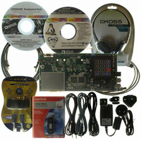
Manufacturer Part Number
ADZS-BF527-EZLITE
Description
BOARD EVAL ADSP-BF527
Manufacturer
Analog Devices Inc
Series
Blackfin®r
Type
DSPr
Datasheet
1.ADZS-BF527-EZLITE.pdf
(80 pages)
Specifications of ADZS-BF527-EZLITE
Featured Product
Blackfin® BF50x Series Processors
Contents
Evaluation Board
Silicon Manufacturer
Analog Devices
Core Architecture
Blackfin
Features
USB-based, PC-hosted Tool Set
Silicon Core Number
ADSP-BF527
Silicon Family Name
Blackfin
Rohs Compliant
Yes
Lead Free Status / RoHS Status
Lead free / RoHS Compliant
For Use With/related Products
ADSP-BF527
Lead Free Status / RoHS Status
Lead free / RoHS Compliant, Lead free / RoHS Compliant


Preliminary Technical Data
Table 9. Fourth Byte for Large Page Devices
Bit
D1:D0 Page Size
D2
D5:D4 Block Size
D6
D3, D7 Not Used for configuration
• Boot from UART0 host on Port G (BMODE = 0x7) —
• Boot from UART1 host on Port F (BMODE = 0x8). Same
• Boot from SDRAM (BMODE = 0xA) This is a warm boot
• Boot from OTP memory (BMODE = 0xB) — This provides
version 2.1. An I
processor at a time when booting multiple processors from
a single TWI.
Using an autobaud handshake sequence, a boot-stream for-
matted program is downloaded by the host. The host
selects a bit rate within the UART clocking capabilities.
When performing the autobaud, the UART expects a “@”
(0x40) character (eight bits data, one start bit, one stop bit,
no parity bit) on the UART0RX pin to determine the bit
rate. The UART then replies with an acknowledgement
composed of 4 bytes (0xBF, the value of UART0_DLL, the
value of UART0_DLH, then 0x00). The host can then
download the boot stream. To hold off the host the Blackfin
processor signals the host with the boot host wait
(HWAIT) signal. Therefore, the host must monitor
HWAIT before every transmitted byte.
as BMODE = 0x7 except that the UART1 port is used.
scenario, where the boot kernel starts booting from address
0x0000 0010. The SDRAM is expected to contain a valid
boot stream and the SDRAM controller must be configured
by the OTP settings.
a stand-alone booting method. The boot stream is loaded
from on-chip OTP memory. By default, the boot stream is
expected to start from OTP page 0x40 and can occupy all
public OTP memory up to page 0xDF. This is 2560 bytes.
Since the start page is programmable, the maximum size of
the boot stream can be extended to 3072 bytes.
Parameter
(excluding spare area)
Spare Area Size
(excluding spare area)
Bus width
2
C multiplexer can be used to select one
Value Meaning
00
01
10
11
00
01
00
01
10
11
00
01
1K byte
2K byte
4K byte
8K byte
8 byte/512 byte
16 byte/512 byte
64K byte
128K byte
256K byte
512K byte
x8
not supported
Rev. PrG | Page 19 of 80 | February 2009
• Boot from 8-bit external NAND flash memory (BMODE =
0xC and BMODE = 0xD) — In this mode, auto detection of
the NAND flash device is performed.
BMODE = 0xC, the processor configures PORTF GPIO
pins PF7:0 for the NAND data pins and PORTH pins
PH15:10 for the NAND control signals.
BMODE = 0xD, the processor configures PORTH GPIO
pins PH7:0 for the NAND data pins and PORTH pins
PH15:10 for the NAND control signals.
For correct device operation pull-up resistors are required
on both ND_CE (PH10) and ND_BUSY (PH13) signals. By
default, a value of 0x0033 is written to the NFC_CTL regis-
ter. The booting procedure always starts by booting from
byte 0 of block 0 of the NAND flash device.
NAND flash boot supports the following features:
Small page NAND flash devices must have a 512-byte page
size, 32 pages per block, a 16-byte spare area size, and a bus
configuration of 8 bits. By default, all read requests from
the NAND flash are followed by four address cycles. If the
NAND flash device requires only three address cycles, the
device must be capable of ignoring the additional address
cycles.
The small page NAND flash device must comply with the
following command set:
For large-page NAND-flash devices, the four-byte elec-
tronic signature is read in order to configure the kernel for
booting, which allows support for multiple large-page
devices. The fourth byte of the electronic signature must
comply with the specification in
Any NAND flash array configuration from
ing 16-bit devices, that also complies with the command set
listed below are directly supported by the boot kernel.
There are no restrictions on the page size or block size as
imposed by the small-page boot kernel.
ADSP-BF522/523/524/525/526/527
—Device Auto Detection
—Error Detection & Correction for maximum reliability
—No boot stream size limitation
—Peripheral DMA providing efficient transfer of all data
—Software-configurable boot mode for booting from
—Software-configurable boot mode for booting from
—Configurable timing via OTP memory
—Reset: 0xFF
—Read lower half of page: 0x00
—Read upper half of page: 0x01
—Read spare area: 0x50
(excluding the ECC parity data)
boot streams spanning multiple blocks, including bad
blocks
multiple copies of the boot stream, allowing for han-
dling of bad blocks and uncorrectable errors
Table
9.
Table
9, exclud-
Related parts for ADZS-BF527-EZLITE
Image
Part Number
Description
Manufacturer
Datasheet
Request
R

Part Number:
Description:
BOARD EVAL MEDIA PLAYER BF527
Manufacturer:
Analog Devices Inc
Datasheet:

Part Number:
Description:
BOARD DAUGHT ADSP-BF533,37,61KIT
Manufacturer:
Analog Devices Inc

Part Number:
Description:
BLACKFIN EZ-EXTENDER Board For ADSP-BF533/61 EZ-KIT LITE
Manufacturer:
Analog Devices Inc

Part Number:
Description:
±1.7g Dual-Axis IMEMS Accelerometer Evaluation Board
Manufacturer:
Analog Devices Inc
Datasheet:

Part Number:
Description:
Inertial Sensor Evaluation System
Manufacturer:
Analog Devices Inc
Datasheet:
Part Number:
Description:
Manufacturer:
Analog Devices Inc
Datasheet:
Part Number:
Description:
Manufacturer:
Analog Devices Inc
Datasheet:
Part Number:
Description:
Manufacturer:
Analog Devices Inc
Datasheet:
Part Number:
Description:
Manufacturer:
Analog Devices Inc
Datasheet:
Part Number:
Description:
Manufacturer:
Analog Devices Inc
Datasheet:
Part Number:
Description:
Manufacturer:
Analog Devices Inc
Datasheet:
Part Number:
Description:
Manufacturer:
Analog Devices Inc
Datasheet:
Part Number:
Description:
Manufacturer:
Analog Devices Inc
Datasheet: