ADZS-BF527-EZLITE Analog Devices Inc, ADZS-BF527-EZLITE Datasheet - Page 28
ADZS-BF527-EZLITE
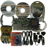
Manufacturer Part Number
ADZS-BF527-EZLITE
Description
BOARD EVAL ADSP-BF527
Manufacturer
Analog Devices Inc
Series
Blackfin®r
Type
DSPr
Datasheet
1.ADZS-BF527-EZLITE.pdf
(80 pages)
Specifications of ADZS-BF527-EZLITE
Featured Product
Blackfin® BF50x Series Processors
Contents
Evaluation Board
Silicon Manufacturer
Analog Devices
Core Architecture
Blackfin
Features
USB-based, PC-hosted Tool Set
Silicon Core Number
ADSP-BF527
Silicon Family Name
Blackfin
Rohs Compliant
Yes
Lead Free Status / RoHS Status
Lead free / RoHS Compliant
For Use With/related Products
ADSP-BF527
Lead Free Status / RoHS Status
Lead free / RoHS Compliant, Lead free / RoHS Compliant


ADSP-BF522/523/524/525/526/527
Table 11
register. Set this register prior to using the TWI port.
Table 11. TWI_DT Field Selections and V
1
ADSP-BF522/524/526 Clock Related Operating Conditions
Table 12
ADSP-BF522/524/526 processors. Take care in selecting MSEL,
SSEL, and CSEL ratios so as not to exceed the maximum core
clock and system clock (see
locked loop operating conditions.
Table 12. Core Clock (CCLK) Requirements—ADSP-BF522/524/526 Processors—All Speed Grades
1
2
3
4
5
Table 13. Phase-Locked Loop Operating Conditions
1
Table 14. ADSP-BF522/524/526 Processors Maximum SCLK Conditions
1
TWI_DT
000 (default)
001
010
011
100
101
110
111 (reserved)
Parameter
f
f
f
f
f
Parameter
f
Parameter
f
f
Designs must comply with the V
See the
Preliminary data indicates a value of 1.33 V.
Applies only to 400 MHz speed grade only. See the
Preliminary data indicates a value of 1.235 V.
Preliminary data indicates a value of 1.14 V.
See the
f
CCLK
CCLK
CCLK
CCLK
CCLK
VCO
SCLK
SCLK
SCLK
must be less than or equal to f
Ordering Guide on Page
Ordering Guide on Page
shows settings for TWI_DT in the NONGPIO_DRIVE
describes the core clock timing requirements for the
1
Core Clock Frequency (V
Core Clock Frequency (V
Core Clock Frequency (V
Core Clock Frequency (V
Core Clock Frequency (V
Voltage Controlled Oscillator (VCO) Frequency
CLKOUT/SCLK Frequency (V
CLKOUT/SCLK Frequency (V
DDEXT
80.
80.
CCLK
Table
and is subject to additional restrictions for SDRAM interface operation. See
V
and V
DDEXT
14).
BUSTWI
3.3
1.8
2.5
1.8
3.3
1.8
2.5
Nominal
–
Table 13
voltages specified for the default TWI_DT setting for correct JTAG boundary scan operation during reset.
Ordering Guide on Page
DDINT
DDINT
DDINT
DDINT
DDINT
DDEXT
DDINT
DDINT
describes phase-
=tbd
=tbd
= tbd
= tbd V minimum)
= tbd V minimum)
/V
Rev. PrG | Page 28 of 80 | February 2009
BUSTWI
tbd V)
tbd V)
2
4
5
V minimum)
V minimum)
V minimum)
V
BUSTWI
1
80.
2.97
2.97
2.97
2.25
2.25
Minimum
1.7
4.5
–
V
DDEXT
Minimum
V
BUSTWI
50
/V
DDMEM
3.3
1.8
3.3
3.3
2.5
2.5
Nominal
5
–
Table 34 on Page
Preliminary Technical Data
= 1.8 V/2.5 V/3.3 V Nominal
tbd
80
1
44.
V
Speed Grade
BUSTWI
Maximum
Max
400
TBD
TBD
350
300
3.63
1.98
3.63
3.63
2.75
2.75
Maximum
5.5
–
3
1
Unit
V
V
V
V
V
V
V
–
MHz
MHz
MHz
MHz
MHz
Unit
MHz
MHz
Unit
MHz
Unit
Related parts for ADZS-BF527-EZLITE
Image
Part Number
Description
Manufacturer
Datasheet
Request
R

Part Number:
Description:
BOARD EVAL MEDIA PLAYER BF527
Manufacturer:
Analog Devices Inc
Datasheet:

Part Number:
Description:
BOARD DAUGHT ADSP-BF533,37,61KIT
Manufacturer:
Analog Devices Inc

Part Number:
Description:
BLACKFIN EZ-EXTENDER Board For ADSP-BF533/61 EZ-KIT LITE
Manufacturer:
Analog Devices Inc

Part Number:
Description:
±1.7g Dual-Axis IMEMS Accelerometer Evaluation Board
Manufacturer:
Analog Devices Inc
Datasheet:

Part Number:
Description:
Inertial Sensor Evaluation System
Manufacturer:
Analog Devices Inc
Datasheet:
Part Number:
Description:
Manufacturer:
Analog Devices Inc
Datasheet:
Part Number:
Description:
Manufacturer:
Analog Devices Inc
Datasheet:
Part Number:
Description:
Manufacturer:
Analog Devices Inc
Datasheet:
Part Number:
Description:
Manufacturer:
Analog Devices Inc
Datasheet:
Part Number:
Description:
Manufacturer:
Analog Devices Inc
Datasheet:
Part Number:
Description:
Manufacturer:
Analog Devices Inc
Datasheet:
Part Number:
Description:
Manufacturer:
Analog Devices Inc
Datasheet:
Part Number:
Description:
Manufacturer:
Analog Devices Inc
Datasheet: