ADZS-BF527-EZLITE Analog Devices Inc, ADZS-BF527-EZLITE Datasheet - Page 5
ADZS-BF527-EZLITE
Manufacturer Part Number
ADZS-BF527-EZLITE
Description
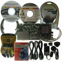
BOARD EVAL ADSP-BF527
Manufacturer
Analog Devices Inc
Series
Blackfin®r
Type
DSPr
Datasheet
1.ADZS-BF527-EZLITE.pdf
(80 pages)
Specifications of ADZS-BF527-EZLITE
Featured Product
Blackfin® BF50x Series Processors
Contents
Evaluation Board
Silicon Manufacturer
Analog Devices
Core Architecture
Blackfin
Features
USB-based, PC-hosted Tool Set
Silicon Core Number
ADSP-BF527
Silicon Family Name
Blackfin
Rohs Compliant
Yes
Lead Free Status / RoHS Status
Lead free / RoHS Compliant
For Use With/related Products
ADSP-BF527
Lead Free Status / RoHS Status
Lead free / RoHS Compliant, Lead free / RoHS Compliant


Preliminary Technical Data
The address arithmetic unit provides two addresses for simulta-
neous dual fetches from memory. It contains a multiported
register file consisting of four sets of 32-bit index, modify,
length, and base registers (for circular buffering), and eight
additional 32-bit pointer registers (for C-style indexed stack
manipulation).
Blackfin processors support a modified Harvard architecture in
combination with a hierarchical memory structure. Level 1 (L1)
memories are those that typically operate at the full processor
speed with little or no latency. At the L1 level, the instruction
memory holds instructions only. The two data memories hold
data, and a dedicated scratchpad data memory stores stack and
local variable information.
In addition, multiple L1 memory blocks are provided, offering a
configurable mix of SRAM and cache. The memory manage-
ment unit (MMU) provides memory protection for individual
tasks that may be operating on the core and can protect system
registers from unintended access.
The architecture provides three modes of operation: user mode,
supervisor mode, and emulation mode. User mode has
restricted access to certain system resources, thus providing a
protected software environment, while supervisor mode has
unrestricted access to the system and core resources.
The Blackfin processor instruction set has been optimized so
that 16-bit opcodes represent the most frequently used instruc-
tions, resulting in excellent compiled code density. Complex
DSP instructions are encoded into 32-bit opcodes, representing
fully featured multifunction instructions. Blackfin processors
support a limited multi-issue capability, where a 32-bit instruc-
tion can be issued in parallel with two 16-bit instructions,
allowing the programmer to use many of the core resources in a
single instruction cycle.
The Blackfin processor assembly language uses an algebraic syn-
tax for ease of coding and readability. The architecture has been
optimized for use in conjunction with the C/C++ compiler,
resulting in fast and efficient software implementations.
MEMORY ARCHITECTURE
The Blackfin processor views memory as a single unified
4G byte address space, using 32-bit addresses. All resources,
including internal memory, external memory, and I/O control
registers, occupy separate sections of this common address
space. The memory portions of this address space are arranged
in a hierarchical structure to provide a good cost/performance
balance of some very fast, low-latency on-chip memory as cache
or SRAM, and larger, lower-cost and performance off-chip
memory systems. See
The on-chip L1 memory system is the highest-performance
memory available to the Blackfin processor. The off-chip mem-
ory system, accessed through the external bus interface unit
(EBIU), provides expansion with SDRAM, flash memory, and
SRAM, optionally accessing up to 132M bytes of
physical memory.
The memory DMA controller provides high-bandwidth data-
movement capability. It can perform block transfers of code or
data between the internal memory and the external
Figure
3.
Rev. PrG | Page 5 of 80 | February 2009
Internal (On-Chip) Memory
The processor has three blocks of on-chip memory providing
high-bandwidth access to the core.
The first block is the L1 instruction memory, consisting of
64K bytes SRAM, of which 16K bytes can be configured as a
four-way set-associative cache. This memory is accessed at full
processor speed.
The second on-chip memory block is the L1 data memory, con-
sisting of up to two banks of up to 32K bytes each. Each memory
bank is configurable, offering both cache and SRAM functional-
ity. This memory block is accessed at full processor speed.
The third memory block is a 4K byte scratchpad SRAM which
runs at the same speed as the L1 memories, but is only accessible
as data SRAM and cannot be configured as cache memory.
External (Off-Chip) Memory
External memory is accessed via the EBIU. This 16-bit interface
provides a glueless connection to a bank of synchronous DRAM
(SDRAM) as well as up to four banks of asynchronous memory
devices including flash, EPROM, ROM, SRAM, and memory
mapped I/O devices.
0xFFFF FFFF
0xFFE0 0000
0xFFC0 0000
0xFFB0 1000
0xFFB0 0000
0xFFA1 4000
0xFFA1 0000
0xFFA0 C000
0xFFA0 8000
0xFFA0 0000
0xFF90 8000
0xFF90 4000
0xFF90 0000
0xFF80 8000
0xFF80 4000
0xFF80 0000
0x08 00 0000
0xEF00 8000
0xEF00 0000
0x2040 0000
0x2030 0000
0x2020 0000
0x2010 0000
0x2000 0000
0x0000 0000
ADSP-BF522/523/524/525/526/527
Figure 3. Internal/External Memory Map
CORE MMR REGISTERS (2M BYTES)
SYSTEM MMR REGISTERS (2M BYTES)
RESERVED
SCRATCHPAD SRAM (4K BYTES)
RESERVED
INSTRUCTION SRAM / CACHE (16K BYTES)
RESERVED
INSTRUCTION BANK B SRAM (16K BYTES)
INSTRUCTION BANK A SRAM (32K BYTES)
RESERVED
DATA BANK B SRAM / CACHE (16K BYTES)
DATA BANK B SRAM (16K BYTES)
RESERVED
DATA BANK A SRAM / CACHE (16K BYTES)
DATA BANK A SRAM (16K BYTES)
RESERVED
BOOT ROM (32K BYTES)
RESERVED
ASYNC MEMORY BANK 3 (1M BYTES)
ASYNC MEMORY BANK 2 (1M BYTES)
ASYNC MEMORY BANK 1 (1M BYTES)
ASYNC MEMORY BANK 0 (1M BYTES)
SDRAM MEMORY (16M BYTES - 128M BYTES)
RESERVED
Related parts for ADZS-BF527-EZLITE
Image
Part Number
Description
Manufacturer
Datasheet
Request
R

Part Number:
Description:
BOARD EVAL MEDIA PLAYER BF527
Manufacturer:
Analog Devices Inc
Datasheet:

Part Number:
Description:
BOARD DAUGHT ADSP-BF533,37,61KIT
Manufacturer:
Analog Devices Inc

Part Number:
Description:
BLACKFIN EZ-EXTENDER Board For ADSP-BF533/61 EZ-KIT LITE
Manufacturer:
Analog Devices Inc

Part Number:
Description:
±1.7g Dual-Axis IMEMS Accelerometer Evaluation Board
Manufacturer:
Analog Devices Inc
Datasheet:

Part Number:
Description:
Inertial Sensor Evaluation System
Manufacturer:
Analog Devices Inc
Datasheet:
Part Number:
Description:
Manufacturer:
Analog Devices Inc
Datasheet:
Part Number:
Description:
Manufacturer:
Analog Devices Inc
Datasheet:
Part Number:
Description:
Manufacturer:
Analog Devices Inc
Datasheet:
Part Number:
Description:
Manufacturer:
Analog Devices Inc
Datasheet:
Part Number:
Description:
Manufacturer:
Analog Devices Inc
Datasheet:
Part Number:
Description:
Manufacturer:
Analog Devices Inc
Datasheet:
Part Number:
Description:
Manufacturer:
Analog Devices Inc
Datasheet:
Part Number:
Description:
Manufacturer:
Analog Devices Inc
Datasheet: