C8051F326DK Silicon Laboratories Inc, C8051F326DK Datasheet - Page 25
C8051F326DK
Manufacturer Part Number
C8051F326DK
Description
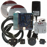
KIT DEV FOR C8051F326/7
Manufacturer
Silicon Laboratories Inc
Type
MCUr
Specifications of C8051F326DK
Contents
Evaluation Board, Power Supply, USB Cables, Adapter and Documentation
Processor To Be Evaluated
C8051F326/F327
Interface Type
USB
Silicon Manufacturer
Silicon Labs
Core Architecture
8051
Silicon Core Number
C8051F326
Silicon Family Name
C8051F32x
Lead Free Status / RoHS Status
Contains lead / RoHS non-compliant
For Use With/related Products
Silicon Laboratories C8051F326, C8051F327
Lead Free Status / Rohs Status
Lead free / RoHS Compliant
Other names
336-1306


4.
REGIN
XTAL2
Pinout and Package Definitions
Name
VBUS
C2CK
P3.0/
P0.3/
GND
RST/
VDD
P0.0
P0.1
P0.2
P0.4
P0.5
C2D
VIO
D+
D–
Pin Numbers
‘F326
10
28
27
26
25
24
6
5
2
9
7
8
3
4
1
Table 4.1. Pin Definitions for the C8051F326/7
‘F327
—
10
28
27
26
25
6
3
9
7
8
4
5
2
1
Power
Power
Power
Power
D I/O
D I/O
D I/O
D I/O
D I/O
D I/O
D I/O
D I/O
D I/O
D I/O
D I/O
D I/O
Type
D In
D In
Out
In
In
In
Description
2.7–3.6 V Core Supply Voltage Input.
3.3 V Voltage Regulator Output. See Section 5.
V I/O Supply Voltage Input. The voltage at this pin must be
less than or equal to the Core Supply Voltage (V
'F326. On the 'F327, this pin is internally connected to V
Ground.
Device Reset. Open-drain output of internal POR or VDD
monitor. An external source can initiate a system reset by
driving this pin low for at least 15 µs. See Section 7.
Clock signal for the C2 Debug Interface.
Port 3.0. See Section 11 for a complete description.
Bi-directional data signal for the C2 Debug Interface.
5 V Regulator Input. This pin is the input to the on-chip volt-
age regulator.
VBUS Sense Input. This pin should be connected to the
VBUS signal of a USB network. A 5 V signal on this pin indi-
cates a USB network connection.
USB D+.
USB D–.
Port 0.0. See Section 11 for a complete description.
Port 0.1. See Section 11 for a complete description.
Port 0.2. See Section 11 for a complete description.
Port 0.3. See Section 11 for a complete description.
External Clock Input. See Section 10 for a complete
description.
Port 0.4. See Section 11 for a complete description.
Port 0.5. See Section 11 for a complete description.
Rev. 1.1
C8051F326/7
DD
) for the
DD
25
.
Related parts for C8051F326DK
Image
Part Number
Description
Manufacturer
Datasheet
Request
R

Part Number:
Description:
SMD/C°/SINGLE-ENDED OUTPUT SILICON OSCILLATOR
Manufacturer:
Silicon Laboratories Inc
Part Number:
Description:
Manufacturer:
Silicon Laboratories Inc
Datasheet:
Part Number:
Description:
N/A N/A/SI4010 AES KEYFOB DEMO WITH LCD RX
Manufacturer:
Silicon Laboratories Inc
Datasheet:
Part Number:
Description:
N/A N/A/SI4010 SIMPLIFIED KEY FOB DEMO WITH LED RX
Manufacturer:
Silicon Laboratories Inc
Datasheet:
Part Number:
Description:
N/A/-40 TO 85 OC/EZLINK MODULE; F930/4432 HIGH BAND (REV E/B1)
Manufacturer:
Silicon Laboratories Inc
Part Number:
Description:
EZLink Module; F930/4432 Low Band (rev e/B1)
Manufacturer:
Silicon Laboratories Inc
Part Number:
Description:
I°/4460 10 DBM RADIO TEST CARD 434 MHZ
Manufacturer:
Silicon Laboratories Inc
Part Number:
Description:
I°/4461 14 DBM RADIO TEST CARD 868 MHZ
Manufacturer:
Silicon Laboratories Inc
Part Number:
Description:
I°/4463 20 DBM RFSWITCH RADIO TEST CARD 460 MHZ
Manufacturer:
Silicon Laboratories Inc
Part Number:
Description:
I°/4463 20 DBM RADIO TEST CARD 868 MHZ
Manufacturer:
Silicon Laboratories Inc
Part Number:
Description:
I°/4463 27 DBM RADIO TEST CARD 868 MHZ
Manufacturer:
Silicon Laboratories Inc
Part Number:
Description:
I°/4463 SKYWORKS 30 DBM RADIO TEST CARD 915 MHZ
Manufacturer:
Silicon Laboratories Inc
Part Number:
Description:
N/A N/A/-40 TO 85 OC/4463 RFMD 30 DBM RADIO TEST CARD 915 MHZ
Manufacturer:
Silicon Laboratories Inc
Part Number:
Description:
I°/4463 20 DBM RADIO TEST CARD 169 MHZ
Manufacturer:
Silicon Laboratories Inc