C8051F326DK Silicon Laboratories Inc, C8051F326DK Datasheet - Page 88
C8051F326DK
Manufacturer Part Number
C8051F326DK
Description
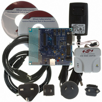
KIT DEV FOR C8051F326/7
Manufacturer
Silicon Laboratories Inc
Type
MCUr
Specifications of C8051F326DK
Contents
Evaluation Board, Power Supply, USB Cables, Adapter and Documentation
Processor To Be Evaluated
C8051F326/F327
Interface Type
USB
Silicon Manufacturer
Silicon Labs
Core Architecture
8051
Silicon Core Number
C8051F326
Silicon Family Name
C8051F32x
Lead Free Status / RoHS Status
Contains lead / RoHS non-compliant
For Use With/related Products
Silicon Laboratories C8051F326, C8051F327
Lead Free Status / Rohs Status
Lead free / RoHS Compliant
Other names
336-1306


C8051F326/7
12.1. Endpoint Addressing
A total of three endpoint pipes are available. The control endpoint (Endpoint0) always functions as a
bi-directional IN/OUT endpoint. Endpoint 1 is implemented as a 64 byte IN pipe and a 128 byte OUT pipe:
12.2. USB Transceiver
The USB Transceiver is configured via the USB0XCN register shown in Figure 12.1. This configuration
includes Transceiver enable/disable, pullup resistor enable/disable, and device speed selection (Full or
Low Speed). When bit SPEED = ‘1’, USB0 operates as a Full Speed USB function, and the on-chip pullup
resistor (if enabled) appears on the D+ pin. When bit SPEED = ‘0’, USB0 operates as a Low Speed USB
function, and the on-chip pullup resistor (if enabled) appears on the D- pin. Bits4-0 of register USB0XCN
can be used for Transceiver testing as described in Figure 12.1. The pullup resistor is enabled only when
VBUS is present (see Section “5.2. VBUS Detection” on page 31 for details on VBUS detection).
Important Note: The USB clock should be active before the Transceiver is enabled.
88
Endpoint0
Endpoint1
Endpoint
Table 12.1. Endpoint Addressing Scheme
Associated Pipes
Endpoint0 OUT
Endpoint1 OUT
Endpoint0 IN
Endpoint1 IN
Rev. 1.1
USB Protocol Address
0x00
0x00
0x81
0x01
Related parts for C8051F326DK
Image
Part Number
Description
Manufacturer
Datasheet
Request
R

Part Number:
Description:
SMD/C°/SINGLE-ENDED OUTPUT SILICON OSCILLATOR
Manufacturer:
Silicon Laboratories Inc
Part Number:
Description:
Manufacturer:
Silicon Laboratories Inc
Datasheet:
Part Number:
Description:
N/A N/A/SI4010 AES KEYFOB DEMO WITH LCD RX
Manufacturer:
Silicon Laboratories Inc
Datasheet:
Part Number:
Description:
N/A N/A/SI4010 SIMPLIFIED KEY FOB DEMO WITH LED RX
Manufacturer:
Silicon Laboratories Inc
Datasheet:
Part Number:
Description:
N/A/-40 TO 85 OC/EZLINK MODULE; F930/4432 HIGH BAND (REV E/B1)
Manufacturer:
Silicon Laboratories Inc
Part Number:
Description:
EZLink Module; F930/4432 Low Band (rev e/B1)
Manufacturer:
Silicon Laboratories Inc
Part Number:
Description:
I°/4460 10 DBM RADIO TEST CARD 434 MHZ
Manufacturer:
Silicon Laboratories Inc
Part Number:
Description:
I°/4461 14 DBM RADIO TEST CARD 868 MHZ
Manufacturer:
Silicon Laboratories Inc
Part Number:
Description:
I°/4463 20 DBM RFSWITCH RADIO TEST CARD 460 MHZ
Manufacturer:
Silicon Laboratories Inc
Part Number:
Description:
I°/4463 20 DBM RADIO TEST CARD 868 MHZ
Manufacturer:
Silicon Laboratories Inc
Part Number:
Description:
I°/4463 27 DBM RADIO TEST CARD 868 MHZ
Manufacturer:
Silicon Laboratories Inc
Part Number:
Description:
I°/4463 SKYWORKS 30 DBM RADIO TEST CARD 915 MHZ
Manufacturer:
Silicon Laboratories Inc
Part Number:
Description:
N/A N/A/-40 TO 85 OC/4463 RFMD 30 DBM RADIO TEST CARD 915 MHZ
Manufacturer:
Silicon Laboratories Inc
Part Number:
Description:
I°/4463 20 DBM RADIO TEST CARD 169 MHZ
Manufacturer:
Silicon Laboratories Inc