C8051F326DK Silicon Laboratories Inc, C8051F326DK Datasheet - Page 64
C8051F326DK
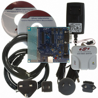
Manufacturer Part Number
C8051F326DK
Description
KIT DEV FOR C8051F326/7
Manufacturer
Silicon Laboratories Inc
Type
MCUr
Specifications of C8051F326DK
Contents
Evaluation Board, Power Supply, USB Cables, Adapter and Documentation
Processor To Be Evaluated
C8051F326/F327
Interface Type
USB
Silicon Manufacturer
Silicon Labs
Core Architecture
8051
Silicon Core Number
C8051F326
Silicon Family Name
C8051F32x
Lead Free Status / RoHS Status
Contains lead / RoHS non-compliant
For Use With/related Products
Silicon Laboratories C8051F326, C8051F327
Lead Free Status / Rohs Status
Lead free / RoHS Compliant
Other names
336-1306


C8051F326/7
8.1.3. Flash Write Procedure
Flash bytes are programmed by software with the following sequence:
Steps 3-8 must be repeated for each byte to be written. After Flash writes are complete, PSWE should be
cleared so that MOVX instructions do not target program memory.
Table 8.1. Flash Electrical Characteristics
64
*Note: 512 bytes at location 0x3E00 to 0x3FFF are reserved.
Erase Cycle Time
Write Cycle Time
Parameter
Endurance
Flash Size
Step 1. Disable interrupts (recommended).
Step 2. Erase the 512-byte Flash page containing the target location, as described in
Step 3. Write the first key code to FLKEY: 0xA5.
Step 4. Write the second key code to FLKEY: 0xF1.
Step 5. Set the PSWE bit (register PSCTL).
Step 6. Clear the PSEE bit (register PSCTL).
Step 7. Using the MOVX instruction, write a single data byte to the desired location within the 512-
Step 8. Clear the PSWE bit (register PSCTL).
Section “8.1.2. Flash Erase Procedure” on page 63.
byte sector.
25 MHz System Clock
25 MHz System Clock
C8051F326/7
Conditions
Rev. 1.1
16384*
Min
20k
10
40
100k
Typ
15
55
—
Max
20
70
—
—
Erase/Write
Units
bytes
ms
µs
Related parts for C8051F326DK
Image
Part Number
Description
Manufacturer
Datasheet
Request
R

Part Number:
Description:
SMD/C°/SINGLE-ENDED OUTPUT SILICON OSCILLATOR
Manufacturer:
Silicon Laboratories Inc
Part Number:
Description:
Manufacturer:
Silicon Laboratories Inc
Datasheet:
Part Number:
Description:
N/A N/A/SI4010 AES KEYFOB DEMO WITH LCD RX
Manufacturer:
Silicon Laboratories Inc
Datasheet:
Part Number:
Description:
N/A N/A/SI4010 SIMPLIFIED KEY FOB DEMO WITH LED RX
Manufacturer:
Silicon Laboratories Inc
Datasheet:
Part Number:
Description:
N/A/-40 TO 85 OC/EZLINK MODULE; F930/4432 HIGH BAND (REV E/B1)
Manufacturer:
Silicon Laboratories Inc
Part Number:
Description:
EZLink Module; F930/4432 Low Band (rev e/B1)
Manufacturer:
Silicon Laboratories Inc
Part Number:
Description:
I°/4460 10 DBM RADIO TEST CARD 434 MHZ
Manufacturer:
Silicon Laboratories Inc
Part Number:
Description:
I°/4461 14 DBM RADIO TEST CARD 868 MHZ
Manufacturer:
Silicon Laboratories Inc
Part Number:
Description:
I°/4463 20 DBM RFSWITCH RADIO TEST CARD 460 MHZ
Manufacturer:
Silicon Laboratories Inc
Part Number:
Description:
I°/4463 20 DBM RADIO TEST CARD 868 MHZ
Manufacturer:
Silicon Laboratories Inc
Part Number:
Description:
I°/4463 27 DBM RADIO TEST CARD 868 MHZ
Manufacturer:
Silicon Laboratories Inc
Part Number:
Description:
I°/4463 SKYWORKS 30 DBM RADIO TEST CARD 915 MHZ
Manufacturer:
Silicon Laboratories Inc
Part Number:
Description:
N/A N/A/-40 TO 85 OC/4463 RFMD 30 DBM RADIO TEST CARD 915 MHZ
Manufacturer:
Silicon Laboratories Inc
Part Number:
Description:
I°/4463 20 DBM RADIO TEST CARD 169 MHZ
Manufacturer:
Silicon Laboratories Inc