C8051T630DK Silicon Laboratories Inc, C8051T630DK Datasheet - Page 15
C8051T630DK
Manufacturer Part Number
C8051T630DK
Description
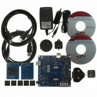
KIT DEV FOR C8051T630 FAMILY
Manufacturer
Silicon Laboratories Inc
Type
MCUr
Specifications of C8051T630DK
Contents
Board, daughter boards, power adapter, cables, documentation and software
Processor To Be Evaluated
C8051T63x
Interface Type
USB
Lead Free Status / RoHS Status
Lead free / RoHS Compliant
For Use With/related Products
C8051T630, T631, T632, T633, T634 and T635 MCUs
For Use With
336-1465 - BOARD SOCKET DAUGHTER 20-QFN
Lead Free Status / Rohs Status
Lead free / RoHS Compliant
Other names
336-1464


1. System Overview
C8051T630/1/2/3/4/5 devices are fully integrated, mixed-signal, system-on-a-chip MCUs. Highlighted fea-
tures are listed below. Refer to Table 2.1 for specific product feature selection and part ordering numbers.
With on-chip power-on reset, V
devices are truly stand-alone, system-on-a-chip solutions. User software has complete control of all
peripherals, and may individually shut down any or all peripherals for power savings.
Code written for the C8051T630/1/2/3/4/5 family of processors will run on the C8051F336 Mixed-Signal
ISP Flash microcontroller, providing a quick, cost-effective way to develop code without requiring special
emulator circuitry. The C8051T630/1/2/3/4/5 processors include Silicon Laboratories’ 2-Wire C2 Debug
and Programming interface, which allows non-intrusive (uses no on-chip resources), full speed, in-circuit
debugging using the production MCU installed in the final application. This debug logic supports inspection
of memory, viewing and modification of special function registers, setting breakpoints, single stepping, and
run and halt commands. All analog and digital peripherals are fully functional while debugging using C2.
The two C2 interface pins can be shared with user functions, allowing in-system debugging without occu-
pying package pins.
Each device is specified for 1.8–3.6 V operation over the industrial temperature range (–45 to +85 °C). An
internal LDO is used to supply the processor core voltage at 1.8 V. The Port I/O and RST pins are tolerant
of input signals up to 5 V. The C8051T630/1/2/3/4/5 are available in 20-pin QFN RoHS compliant packag-
ing. See Table 2.1 for ordering information. A block diagram is shown in Figure 1.1.
High-speed pipelined 8051-compatible microcontroller core (up to 25 MIPS)
In-system, full-speed, non-intrusive debug interface (on-chip)
C8051F336 ISP Flash device is available for quick in-system code development
10-bit 500 ksps Single-ended ADC with analog multiplexer and integrated temperature sensor
10-bit Current Output DAC
Precision calibrated 24.5 MHz internal oscillator
8/4/2 kB of on-chip Byte-Programmable EPROM—(512 bytes are reserved on 8k version)
768 bytes of on-chip RAM
SMBus/I2C, Enhanced UART, and Enhanced SPI serial interfaces implemented in hardware
Four general-purpose 16-bit timers
Programmable Counter/Timer Array (PCA) with three capture/compare modules and Watchdog Timer
function
On-chip Power-On Reset, V
On-chip Voltage Comparator
17 Port I/O
DD
DD
Monitor, and Temperature Sensor
monitor, watchdog timer, and clock oscillator, the C8051T630/1/2/3/4/5
Rev. 1.0
C8051T630/1/2/3/4/5
15
Related parts for C8051T630DK
Image
Part Number
Description
Manufacturer
Datasheet
Request
R

Part Number:
Description:
SMD/C°/SINGLE-ENDED OUTPUT SILICON OSCILLATOR
Manufacturer:
Silicon Laboratories Inc
Part Number:
Description:
Manufacturer:
Silicon Laboratories Inc
Datasheet:
Part Number:
Description:
N/A N/A/SI4010 AES KEYFOB DEMO WITH LCD RX
Manufacturer:
Silicon Laboratories Inc
Datasheet:
Part Number:
Description:
N/A N/A/SI4010 SIMPLIFIED KEY FOB DEMO WITH LED RX
Manufacturer:
Silicon Laboratories Inc
Datasheet:
Part Number:
Description:
N/A/-40 TO 85 OC/EZLINK MODULE; F930/4432 HIGH BAND (REV E/B1)
Manufacturer:
Silicon Laboratories Inc
Part Number:
Description:
EZLink Module; F930/4432 Low Band (rev e/B1)
Manufacturer:
Silicon Laboratories Inc
Part Number:
Description:
I°/4460 10 DBM RADIO TEST CARD 434 MHZ
Manufacturer:
Silicon Laboratories Inc
Part Number:
Description:
I°/4461 14 DBM RADIO TEST CARD 868 MHZ
Manufacturer:
Silicon Laboratories Inc
Part Number:
Description:
I°/4463 20 DBM RFSWITCH RADIO TEST CARD 460 MHZ
Manufacturer:
Silicon Laboratories Inc
Part Number:
Description:
I°/4463 20 DBM RADIO TEST CARD 868 MHZ
Manufacturer:
Silicon Laboratories Inc
Part Number:
Description:
I°/4463 27 DBM RADIO TEST CARD 868 MHZ
Manufacturer:
Silicon Laboratories Inc
Part Number:
Description:
I°/4463 SKYWORKS 30 DBM RADIO TEST CARD 915 MHZ
Manufacturer:
Silicon Laboratories Inc
Part Number:
Description:
N/A N/A/-40 TO 85 OC/4463 RFMD 30 DBM RADIO TEST CARD 915 MHZ
Manufacturer:
Silicon Laboratories Inc
Part Number:
Description:
I°/4463 20 DBM RADIO TEST CARD 169 MHZ
Manufacturer:
Silicon Laboratories Inc