C8051T630DK Silicon Laboratories Inc, C8051T630DK Datasheet - Page 198
C8051T630DK
Manufacturer Part Number
C8051T630DK
Description
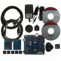
KIT DEV FOR C8051T630 FAMILY
Manufacturer
Silicon Laboratories Inc
Type
MCUr
Specifications of C8051T630DK
Contents
Board, daughter boards, power adapter, cables, documentation and software
Processor To Be Evaluated
C8051T63x
Interface Type
USB
Lead Free Status / RoHS Status
Lead free / RoHS Compliant
For Use With/related Products
C8051T630, T631, T632, T633, T634 and T635 MCUs
For Use With
336-1465 - BOARD SOCKET DAUGHTER 20-QFN
Lead Free Status / Rohs Status
Lead free / RoHS Compliant
Other names
336-1464


C8051T630/1/2/3/4/5
25.3.4. Frequency Output Mode
Frequency Output Mode produces a programmable-frequency square wave on the module’s associated
CEXn pin. The capture/compare module high byte holds the number of PCA clocks to count before the out-
put is toggled. The frequency of the square wave is then defined by Equation 25.1.
Where F
PCA0MD. The lower byte of the capture/compare module is compared to the PCA counter low byte; on a
match, CEXn is toggled and the offset held in the high byte is added to the matched value in PCA0CPLn.
Frequency Output Mode is enabled by setting the ECOMn, TOGn, and PWMn bits in the PCA0CPMn reg-
ister. Note that the MATn bit should normally be set to 0 in this mode. If the MATn bit is set to 1, the CCFn
flag for the channel will be set when the 16-bit PCA0 counter and the 16-bit capture/compare register for
the channel are equal.
25.3.5. 8-bit, 9-bit, 10-bit and 11-bit Pulse Width Modulator Modes
Each module can be used independently to generate a pulse width modulated (PWM) output on its associ-
ated CEXn pin. The frequency of the output is dependent on the timebase for the PCA counter/timer, and
the setting of the PWM cycle length (8, 9, 10 or 11-bits). For backwards-compatibility with the 8-bit PWM
mode available on other devices, the 8-bit PWM mode operates slightly different than 9, 10 and 11-bit
PWM modes. It is important to note that all channels configured for 8/9/10/11-bit PWM mode will use
the same cycle length. It is not possible to configure one channel for 8-bit PWM mode and another for 11-
bit mode (for example). However, other PCA channels can be configured to Pin Capture, High-Speed Out-
put, Software Timer, Frequency Output, or 16-bit PWM mode independently.
198
Note: A value of 0x00 in the PCA0CPHn register is equal to 256 for this equation.
PCA0CPLn
Write to
Reset
PCA0CPHn
PCA
Write to
is the frequency of the clock selected by the CPS2–0 bits in the PCA mode register,
0
ENB
ENB
1
Equation 25.1. Square Wave Frequency Output
W
M
Figure 25.7. PCA Frequency Output Mode
P
1
6
n
x
E
C
O
M
n
PCA0CPMn
C
A
P
P
n
0 0 0
C
A
P
N
n
M
A
T
n
O
G
T
n
W
M
P
n
E
C
C
F
n
x
PCA Timebase
F
CEXn
Enable
=
---------------------------------------- -
2
Rev. 1.0
Comparator
PCA0CPLn
PCA0L
8-bit
PCA0CPHn
F
PCA
match
Enable
Adder
8-bit Adder
Toggle
TOGn
0
1
CEXn
PCA0CPHn
Crossbar
Port I/O
Related parts for C8051T630DK
Image
Part Number
Description
Manufacturer
Datasheet
Request
R

Part Number:
Description:
SMD/C°/SINGLE-ENDED OUTPUT SILICON OSCILLATOR
Manufacturer:
Silicon Laboratories Inc
Part Number:
Description:
Manufacturer:
Silicon Laboratories Inc
Datasheet:
Part Number:
Description:
N/A N/A/SI4010 AES KEYFOB DEMO WITH LCD RX
Manufacturer:
Silicon Laboratories Inc
Datasheet:
Part Number:
Description:
N/A N/A/SI4010 SIMPLIFIED KEY FOB DEMO WITH LED RX
Manufacturer:
Silicon Laboratories Inc
Datasheet:
Part Number:
Description:
N/A/-40 TO 85 OC/EZLINK MODULE; F930/4432 HIGH BAND (REV E/B1)
Manufacturer:
Silicon Laboratories Inc
Part Number:
Description:
EZLink Module; F930/4432 Low Band (rev e/B1)
Manufacturer:
Silicon Laboratories Inc
Part Number:
Description:
I°/4460 10 DBM RADIO TEST CARD 434 MHZ
Manufacturer:
Silicon Laboratories Inc
Part Number:
Description:
I°/4461 14 DBM RADIO TEST CARD 868 MHZ
Manufacturer:
Silicon Laboratories Inc
Part Number:
Description:
I°/4463 20 DBM RFSWITCH RADIO TEST CARD 460 MHZ
Manufacturer:
Silicon Laboratories Inc
Part Number:
Description:
I°/4463 20 DBM RADIO TEST CARD 868 MHZ
Manufacturer:
Silicon Laboratories Inc
Part Number:
Description:
I°/4463 27 DBM RADIO TEST CARD 868 MHZ
Manufacturer:
Silicon Laboratories Inc
Part Number:
Description:
I°/4463 SKYWORKS 30 DBM RADIO TEST CARD 915 MHZ
Manufacturer:
Silicon Laboratories Inc
Part Number:
Description:
N/A N/A/-40 TO 85 OC/4463 RFMD 30 DBM RADIO TEST CARD 915 MHZ
Manufacturer:
Silicon Laboratories Inc
Part Number:
Description:
I°/4463 20 DBM RADIO TEST CARD 169 MHZ
Manufacturer:
Silicon Laboratories Inc