C8051T630DK Silicon Laboratories Inc, C8051T630DK Datasheet - Page 8
C8051T630DK
Manufacturer Part Number
C8051T630DK
Description
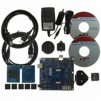
KIT DEV FOR C8051T630 FAMILY
Manufacturer
Silicon Laboratories Inc
Type
MCUr
Specifications of C8051T630DK
Contents
Board, daughter boards, power adapter, cables, documentation and software
Processor To Be Evaluated
C8051T63x
Interface Type
USB
Lead Free Status / RoHS Status
Lead free / RoHS Compliant
For Use With/related Products
C8051T630, T631, T632, T633, T634 and T635 MCUs
For Use With
336-1465 - BOARD SOCKET DAUGHTER 20-QFN
Lead Free Status / Rohs Status
Lead free / RoHS Compliant
Other names
336-1464


C8051T630/1/2/3/4/5
21. SMBus
22. UART0
23. Enhanced Serial Peripheral Interface (SPI0)
24. Timers
25. Programmable Counter Array
8
Figure 20.4. Crossbar Priority Decoder with Crystal Pins Skipped ....................... 115
Figure 21.1. SMBus Block Diagram ...................................................................... 127
Figure 21.2. Typical SMBus Configuration ............................................................ 128
Figure 21.3. SMBus Transaction ........................................................................... 129
Figure 21.4. Typical SMBus SCL Generation ........................................................ 131
Figure 21.5. Typical Master Write Sequence ........................................................ 140
Figure 21.6. Typical Master Read Sequence ........................................................ 141
Figure 21.7. Typical Slave Write Sequence .......................................................... 142
Figure 21.8. Typical Slave Read Sequence .......................................................... 143
Figure 22.1. UART0 Block Diagram ...................................................................... 148
Figure 22.2. UART0 Baud Rate Logic ................................................................... 149
Figure 22.3. UART Interconnect Diagram ............................................................. 150
Figure 22.4. 8-Bit UART Timing Diagram .............................................................. 150
Figure 22.5. 9-Bit UART Timing Diagram .............................................................. 151
Figure 22.6. UART Multi-Processor Mode Interconnect Diagram ......................... 152
Figure 23.1. SPI Block Diagram ............................................................................ 156
Figure 23.2. Multiple-Master Mode Connection Diagram ...................................... 158
Figure 23.3. 3-Wire Single Master and 3-Wire
Figure 23.4. 4-Wire Single Master Mode
Figure 23.5. Master Mode Data/Clock Timing ....................................................... 161
Figure 23.6. Slave Mode Data/Clock Timing (CKPHA = 0) ................................... 161
Figure 23.7. Slave Mode Data/Clock Timing (CKPHA = 1) ................................... 162
Figure 23.8. SPI Master Timing (CKPHA = 0) ....................................................... 166
Figure 23.9. SPI Master Timing (CKPHA = 1) ....................................................... 166
Figure 23.10. SPI Slave Timing (CKPHA = 0) ....................................................... 167
Figure 23.11. SPI Slave Timing (CKPHA = 1) ....................................................... 167
Figure 24.1. T0 Mode 0 Block Diagram ................................................................. 172
Figure 24.2. T0 Mode 2 Block Diagram ................................................................. 173
Figure 24.3. T0 Mode 3 Block Diagram ................................................................. 174
Figure 24.4. Timer 2 16-Bit Mode Block Diagram ................................................. 179
Figure 24.5. Timer 2 8-Bit Mode Block Diagram ................................................... 180
Figure 24.6. Timer 2 Low-Frequency Oscillation Capture Mode Block Diagram ... 181
Figure 24.7. Timer 3 16-Bit Mode Block Diagram ................................................. 185
Figure 24.8. Timer 3 8-Bit Mode Block Diagram ................................................... 186
Figure 24.9. Timer 3 Low-Frequency Oscillation Capture Mode Block Diagram ... 187
Figure 25.1. PCA Block Diagram ........................................................................... 191
Figure 25.2. PCA Counter/Timer Block Diagram ................................................... 192
Figure 25.3. PCA Interrupt Block Diagram ............................................................ 193
Single Slave Mode Connection Diagram .......................................... 159
and 4-Wire Slave Mode Connection Diagram ................................... 159
Rev. 1.0
Related parts for C8051T630DK
Image
Part Number
Description
Manufacturer
Datasheet
Request
R

Part Number:
Description:
SMD/C°/SINGLE-ENDED OUTPUT SILICON OSCILLATOR
Manufacturer:
Silicon Laboratories Inc
Part Number:
Description:
Manufacturer:
Silicon Laboratories Inc
Datasheet:
Part Number:
Description:
N/A N/A/SI4010 AES KEYFOB DEMO WITH LCD RX
Manufacturer:
Silicon Laboratories Inc
Datasheet:
Part Number:
Description:
N/A N/A/SI4010 SIMPLIFIED KEY FOB DEMO WITH LED RX
Manufacturer:
Silicon Laboratories Inc
Datasheet:
Part Number:
Description:
N/A/-40 TO 85 OC/EZLINK MODULE; F930/4432 HIGH BAND (REV E/B1)
Manufacturer:
Silicon Laboratories Inc
Part Number:
Description:
EZLink Module; F930/4432 Low Band (rev e/B1)
Manufacturer:
Silicon Laboratories Inc
Part Number:
Description:
I°/4460 10 DBM RADIO TEST CARD 434 MHZ
Manufacturer:
Silicon Laboratories Inc
Part Number:
Description:
I°/4461 14 DBM RADIO TEST CARD 868 MHZ
Manufacturer:
Silicon Laboratories Inc
Part Number:
Description:
I°/4463 20 DBM RFSWITCH RADIO TEST CARD 460 MHZ
Manufacturer:
Silicon Laboratories Inc
Part Number:
Description:
I°/4463 20 DBM RADIO TEST CARD 868 MHZ
Manufacturer:
Silicon Laboratories Inc
Part Number:
Description:
I°/4463 27 DBM RADIO TEST CARD 868 MHZ
Manufacturer:
Silicon Laboratories Inc
Part Number:
Description:
I°/4463 SKYWORKS 30 DBM RADIO TEST CARD 915 MHZ
Manufacturer:
Silicon Laboratories Inc
Part Number:
Description:
N/A N/A/-40 TO 85 OC/4463 RFMD 30 DBM RADIO TEST CARD 915 MHZ
Manufacturer:
Silicon Laboratories Inc
Part Number:
Description:
I°/4463 20 DBM RADIO TEST CARD 169 MHZ
Manufacturer:
Silicon Laboratories Inc