C8051T630DK Silicon Laboratories Inc, C8051T630DK Datasheet - Page 33
C8051T630DK
Manufacturer Part Number
C8051T630DK
Description
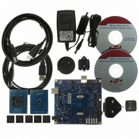
KIT DEV FOR C8051T630 FAMILY
Manufacturer
Silicon Laboratories Inc
Type
MCUr
Specifications of C8051T630DK
Contents
Board, daughter boards, power adapter, cables, documentation and software
Processor To Be Evaluated
C8051T63x
Interface Type
USB
Lead Free Status / RoHS Status
Lead free / RoHS Compliant
For Use With/related Products
C8051T630, T631, T632, T633, T634 and T635 MCUs
For Use With
336-1465 - BOARD SOCKET DAUGHTER 20-QFN
Lead Free Status / Rohs Status
Lead free / RoHS Compliant
Other names
336-1464


6. 10-Bit ADC (ADC0, C8051T630/2/4 only)
ADC0 on the C8051T630/2/4 is a 500 ksps, 10-bit successive-approximation-register (SAR) ADC with
integrated track-and-hold, a gain stage programmable to 1x or 0.5x, and a programmable window detector.
The ADC is fully configurable under software control via Special Function Registers. The ADC may be con-
figured to measure various different signals using the analog multiplexer described in Section “6.5. ADC0
Analog Multiplexer (C8051T630/2/4 only)” on page 43. The voltage reference for the ADC is selected as
described in Section “9. Voltage Reference Options” on page 52. The ADC0 subsystem is enabled only
when the AD0EN bit in the ADC0 Control register (ADC0CN) is set to logic 1. The ADC0 subsystem is in
low power shutdown when this bit is logic 0.
AMUX0
From
X1 or
X0.5
AMP0GN0
Figure 6.1. ADC0 Functional Block Diagram
AIN
ADC0CF
ADC
10-Bit
VDD
SAR
Rev. 1.0
ADC0GTH ADC0GTL
ADC0LTH
ADC0CN
C8051T630/1/2/3/4/5
ADC0LTL
Conversion
Start
000
001
010
011
100
101
32
AD0WINT
Compare
Window
CNVSTR Input
AD0BUSY (W)
Timer 0 Overflow
Timer 2 Overflow
Timer 1 Overflow
Timer 3 Overflow
Logic
33
Related parts for C8051T630DK
Image
Part Number
Description
Manufacturer
Datasheet
Request
R

Part Number:
Description:
SMD/C°/SINGLE-ENDED OUTPUT SILICON OSCILLATOR
Manufacturer:
Silicon Laboratories Inc
Part Number:
Description:
Manufacturer:
Silicon Laboratories Inc
Datasheet:
Part Number:
Description:
N/A N/A/SI4010 AES KEYFOB DEMO WITH LCD RX
Manufacturer:
Silicon Laboratories Inc
Datasheet:
Part Number:
Description:
N/A N/A/SI4010 SIMPLIFIED KEY FOB DEMO WITH LED RX
Manufacturer:
Silicon Laboratories Inc
Datasheet:
Part Number:
Description:
N/A/-40 TO 85 OC/EZLINK MODULE; F930/4432 HIGH BAND (REV E/B1)
Manufacturer:
Silicon Laboratories Inc
Part Number:
Description:
EZLink Module; F930/4432 Low Band (rev e/B1)
Manufacturer:
Silicon Laboratories Inc
Part Number:
Description:
I°/4460 10 DBM RADIO TEST CARD 434 MHZ
Manufacturer:
Silicon Laboratories Inc
Part Number:
Description:
I°/4461 14 DBM RADIO TEST CARD 868 MHZ
Manufacturer:
Silicon Laboratories Inc
Part Number:
Description:
I°/4463 20 DBM RFSWITCH RADIO TEST CARD 460 MHZ
Manufacturer:
Silicon Laboratories Inc
Part Number:
Description:
I°/4463 20 DBM RADIO TEST CARD 868 MHZ
Manufacturer:
Silicon Laboratories Inc
Part Number:
Description:
I°/4463 27 DBM RADIO TEST CARD 868 MHZ
Manufacturer:
Silicon Laboratories Inc
Part Number:
Description:
I°/4463 SKYWORKS 30 DBM RADIO TEST CARD 915 MHZ
Manufacturer:
Silicon Laboratories Inc
Part Number:
Description:
N/A N/A/-40 TO 85 OC/4463 RFMD 30 DBM RADIO TEST CARD 915 MHZ
Manufacturer:
Silicon Laboratories Inc
Part Number:
Description:
I°/4463 20 DBM RADIO TEST CARD 169 MHZ
Manufacturer:
Silicon Laboratories Inc