C8051T630DK Silicon Laboratories Inc, C8051T630DK Datasheet - Page 52
C8051T630DK
Manufacturer Part Number
C8051T630DK
Description
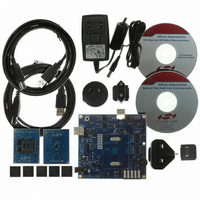
KIT DEV FOR C8051T630 FAMILY
Manufacturer
Silicon Laboratories Inc
Type
MCUr
Specifications of C8051T630DK
Contents
Board, daughter boards, power adapter, cables, documentation and software
Processor To Be Evaluated
C8051T63x
Interface Type
USB
Lead Free Status / RoHS Status
Lead free / RoHS Compliant
For Use With/related Products
C8051T630, T631, T632, T633, T634 and T635 MCUs
For Use With
336-1465 - BOARD SOCKET DAUGHTER 20-QFN
Lead Free Status / Rohs Status
Lead free / RoHS Compliant
Other names
336-1464


C8051T630/1/2/3/4/5
9. Voltage Reference Options
The Voltage reference multiplexer for the ADC is configurable to use an externally connected voltage refer-
ence, the on-chip reference voltage generator routed to the VREF pin, the unregulated power supply volt-
age (V
), or the regulated 1.8 V internal supply (see Figure 9.1). The REFSL bit in the Reference Control
DD
register (REF0CN, SFR Definition 9.1) selects the reference source for the ADC. For an external source or
the on-chip reference, REFSL should be set to 0 to select the VREF pin. To use V
as the reference
DD
source, REFSL should be set to 1. To override this selection and use the internal regulator as the reference
source, the REGOVR bit can be set to 1.
The BIASE bit enables the internal voltage bias generator, which is used by many of the analog peripherals
on the device. This bias is automatically enabled when any peripheral which requires it is enabled, and it
does not need to be enabled manually. The bias generator may be enabled manually by writing a 1 to the
BIASE bit in register REF0CN. The electrical specifications for the voltage reference circuit are given in
Table 5.11.
The C8051T630/2/4 devices also include an on-chip voltage reference circuit which consists of a 1.2 V,
temperature stable bandgap voltage reference generator and a selectable-gain output buffer amplifier. The
buffer is configured for 1x or 2x gain using the REFBGS bit in register REF0CN. On the 1x gain setting the
output voltage is nominally 1.2 V, and on the 2x gain setting the output voltage is nominally 2.4 V. The on-
chip voltage reference can be driven on the VREF pin by setting the REFBE bit in register REF0CN to a 1.
The maximum load seen by the VREF pin must be less than 200 µA to GND. Bypass capacitors of 0.1 µF
and 4.7 µF are recommended from the VREF pin to GND, and a minimum of 0.1uF is required. If the on-
chip reference is not used, the REFBE bit should be cleared to 0. Electrical specifications for the on-chip
voltage reference are given in Table 5.11.
Important Note about the VREF Pin: When using either an external voltage reference or the on-chip ref-
erence circuitry, the VREF pin should be configured as an analog pin and skipped by the Digital Crossbar.
Refer to Section “20. Port Input/Output” on page 109 for the location of the VREF pin, as well as details of
how to configure the pin in analog mode and to be skipped by the crossbar.
52
Rev. 1.0
Related parts for C8051T630DK
Image
Part Number
Description
Manufacturer
Datasheet
Request
R

Part Number:
Description:
SMD/C°/SINGLE-ENDED OUTPUT SILICON OSCILLATOR
Manufacturer:
Silicon Laboratories Inc
Part Number:
Description:
Manufacturer:
Silicon Laboratories Inc
Datasheet:
Part Number:
Description:
N/A N/A/SI4010 AES KEYFOB DEMO WITH LCD RX
Manufacturer:
Silicon Laboratories Inc
Datasheet:
Part Number:
Description:
N/A N/A/SI4010 SIMPLIFIED KEY FOB DEMO WITH LED RX
Manufacturer:
Silicon Laboratories Inc
Datasheet:
Part Number:
Description:
N/A/-40 TO 85 OC/EZLINK MODULE; F930/4432 HIGH BAND (REV E/B1)
Manufacturer:
Silicon Laboratories Inc
Part Number:
Description:
EZLink Module; F930/4432 Low Band (rev e/B1)
Manufacturer:
Silicon Laboratories Inc
Part Number:
Description:
I°/4460 10 DBM RADIO TEST CARD 434 MHZ
Manufacturer:
Silicon Laboratories Inc
Part Number:
Description:
I°/4461 14 DBM RADIO TEST CARD 868 MHZ
Manufacturer:
Silicon Laboratories Inc
Part Number:
Description:
I°/4463 20 DBM RFSWITCH RADIO TEST CARD 460 MHZ
Manufacturer:
Silicon Laboratories Inc
Part Number:
Description:
I°/4463 20 DBM RADIO TEST CARD 868 MHZ
Manufacturer:
Silicon Laboratories Inc
Part Number:
Description:
I°/4463 27 DBM RADIO TEST CARD 868 MHZ
Manufacturer:
Silicon Laboratories Inc
Part Number:
Description:
I°/4463 SKYWORKS 30 DBM RADIO TEST CARD 915 MHZ
Manufacturer:
Silicon Laboratories Inc
Part Number:
Description:
N/A N/A/-40 TO 85 OC/4463 RFMD 30 DBM RADIO TEST CARD 915 MHZ
Manufacturer:
Silicon Laboratories Inc
Part Number:
Description:
I°/4463 20 DBM RADIO TEST CARD 169 MHZ
Manufacturer:
Silicon Laboratories Inc