C8051T630DK Silicon Laboratories Inc, C8051T630DK Datasheet - Page 4
C8051T630DK
Manufacturer Part Number
C8051T630DK
Description
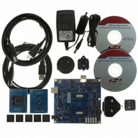
KIT DEV FOR C8051T630 FAMILY
Manufacturer
Silicon Laboratories Inc
Type
MCUr
Specifications of C8051T630DK
Contents
Board, daughter boards, power adapter, cables, documentation and software
Processor To Be Evaluated
C8051T63x
Interface Type
USB
Lead Free Status / RoHS Status
Lead free / RoHS Compliant
For Use With/related Products
C8051T630, T631, T632, T633, T634 and T635 MCUs
For Use With
336-1465 - BOARD SOCKET DAUGHTER 20-QFN
Lead Free Status / Rohs Status
Lead free / RoHS Compliant
Other names
336-1464


C8051T630/1/2/3/4/5
15. Interrupts ................................................................................................................ 80
16. EPROM Memory ..................................................................................................... 89
17. Power Management Modes................................................................................... 92
18. Reset Sources ........................................................................................................ 95
19. Oscillators and Clock Selection ......................................................................... 101
20. Port Input/Output ................................................................................................. 109
4
15.1. MCU Interrupt Sources and Vectors................................................................ 81
15.2. Interrupt Register Descriptions ........................................................................ 82
15.3. INT0 and INT1 External Interrupts................................................................... 87
16.1. Programming and Reading the EPROM Memory ........................................... 89
16.2. Security Options .............................................................................................. 90
16.3. Program Memory CRC .................................................................................... 91
17.1. Idle Mode......................................................................................................... 92
17.2. Stop Mode ....................................................................................................... 93
17.3. Suspend Mode ................................................................................................ 93
18.1. Power-On Reset .............................................................................................. 96
18.2. Power-Fail Reset/VDD Monitor ....................................................................... 97
18.3. External Reset ................................................................................................. 98
18.4. Missing Clock Detector Reset ......................................................................... 98
18.5. Comparator0 Reset ......................................................................................... 99
18.6. PCA Watchdog Timer Reset ........................................................................... 99
18.7. EPROM Error Reset ........................................................................................ 99
18.8. Software Reset ................................................................................................ 99
19.1. System Clock Selection................................................................................. 101
19.2. Programmable Internal High-Frequency (H-F) Oscillator .............................. 103
19.3. Programmable Internal Low-Frequency (L-F) Oscillator ............................... 105
19.4. External Oscillator Drive Circuit..................................................................... 106
20.1. Port I/O Modes of Operation.......................................................................... 110
20.2. Assigning Port I/O Pins to Analog and Digital Functions............................... 112
15.1.1. Interrupt Priorities.................................................................................... 81
15.1.2. Interrupt Latency ..................................................................................... 81
16.1.1. EPROM Write Procedure ........................................................................ 89
16.1.2. EPROM Read Procedure........................................................................ 90
16.3.1. Performing 32-bit CRCs on Full EPROM Content .................................. 91
16.3.2. Performing 16-bit CRCs on 256-Byte EPROM Blocks............................ 91
19.2.1. Internal Oscillator Suspend Mode ......................................................... 103
19.3.1. Calibrating the Internal L-F Oscillator.................................................... 105
19.4.1. External RC Example............................................................................ 108
19.4.2. External Capacitor Example.................................................................. 108
20.1.1. Port Pins Configured for Analog I/O...................................................... 110
20.1.2. Port Pins Configured For Digital I/O...................................................... 110
20.1.3. Interfacing Port I/O to 5V Logic ............................................................. 111
20.2.1. Assigning Port I/O Pins to Analog Functions ........................................ 112
20.2.2. Assigning Port I/O Pins to Digital Functions.......................................... 112
20.2.3. Assigning Port I/O Pins to External Digital Event Capture Functions ... 113
Rev. 1.0
Related parts for C8051T630DK
Image
Part Number
Description
Manufacturer
Datasheet
Request
R

Part Number:
Description:
SMD/C°/SINGLE-ENDED OUTPUT SILICON OSCILLATOR
Manufacturer:
Silicon Laboratories Inc
Part Number:
Description:
Manufacturer:
Silicon Laboratories Inc
Datasheet:
Part Number:
Description:
N/A N/A/SI4010 AES KEYFOB DEMO WITH LCD RX
Manufacturer:
Silicon Laboratories Inc
Datasheet:
Part Number:
Description:
N/A N/A/SI4010 SIMPLIFIED KEY FOB DEMO WITH LED RX
Manufacturer:
Silicon Laboratories Inc
Datasheet:
Part Number:
Description:
N/A/-40 TO 85 OC/EZLINK MODULE; F930/4432 HIGH BAND (REV E/B1)
Manufacturer:
Silicon Laboratories Inc
Part Number:
Description:
EZLink Module; F930/4432 Low Band (rev e/B1)
Manufacturer:
Silicon Laboratories Inc
Part Number:
Description:
I°/4460 10 DBM RADIO TEST CARD 434 MHZ
Manufacturer:
Silicon Laboratories Inc
Part Number:
Description:
I°/4461 14 DBM RADIO TEST CARD 868 MHZ
Manufacturer:
Silicon Laboratories Inc
Part Number:
Description:
I°/4463 20 DBM RFSWITCH RADIO TEST CARD 460 MHZ
Manufacturer:
Silicon Laboratories Inc
Part Number:
Description:
I°/4463 20 DBM RADIO TEST CARD 868 MHZ
Manufacturer:
Silicon Laboratories Inc
Part Number:
Description:
I°/4463 27 DBM RADIO TEST CARD 868 MHZ
Manufacturer:
Silicon Laboratories Inc
Part Number:
Description:
I°/4463 SKYWORKS 30 DBM RADIO TEST CARD 915 MHZ
Manufacturer:
Silicon Laboratories Inc
Part Number:
Description:
N/A N/A/-40 TO 85 OC/4463 RFMD 30 DBM RADIO TEST CARD 915 MHZ
Manufacturer:
Silicon Laboratories Inc
Part Number:
Description:
I°/4463 20 DBM RADIO TEST CARD 169 MHZ
Manufacturer:
Silicon Laboratories Inc